Used ESI / MICROVISION 3900 #9255776 for sale
URL successfully copied!
Tap to zoom


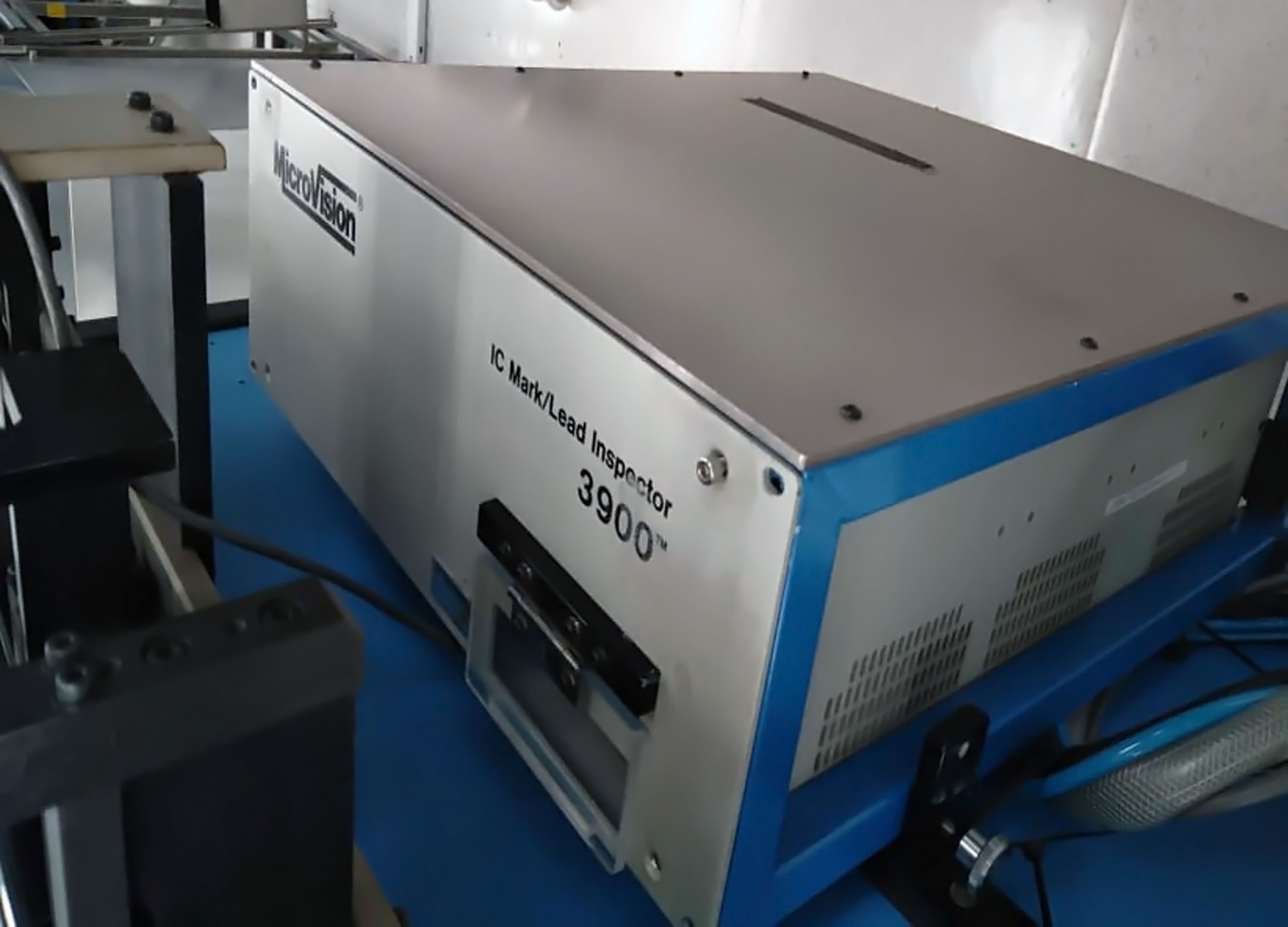
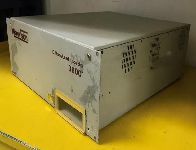
ESI / MICROVISION 3900 is a complete mask and wafer inspection equipment that combines precise imaging, advanced defect review, and in-depth data analysis to deliver the robust defect detection and classification needed for advanced semiconductor processes. This system takes advantage of advanced optics, intelligent algorithm technology, and a wide range of digital image capture and analysis tools to provide fast and reliable inspection of masks and wafers. The mask and wafer are scanned by ESI 3900's automated high-resolution lens unit. The lens machine includes a portable camera with manual or automatic zoom, focus and exposure adjustment. This helps to optimize the image magnification for both mask and wafer inspection. It also features an onboard monitor that displays the images in various modes for quick determination of defects. MICROVISION 3900 offers high-speed mask and wafer inspection with digital imaging techniques and advanced defect detection algorithms. This enables the tool to locate small, difficult-to-detect defects quickly and accurately. It can even detect defects at multiple magnifications, allowing engineers to quickly find the most trouble-prone sections of a given product. 3900 is designed with advanced wafer inspection capabilities. It quickly and accurately analyses the entire range of wafer layout features, from coarse to ultra-fine. It can also inspect and detect lithography defects, particle and contamination, resistivity and surface topography. ESI / MICROVISION 3900 utilizes a flexible graphical user interface, adjustable workflows, and powerful image analysis tools to streamline data processing. It also supports advanced automation options including programmable data storage and retrieval, automated defect detection, and defect classification. This eliminates the rescanning of large images and allows for fast and precise defect classification. Overall, ESI 3900 is one of the most reliable and efficient mask and wafer inspection systems currently available. It is well-suited for advanced semiconductor processes that require high-speed, high-resolution imaging. Its capabilities allow engineers to quickly find hard-to-detect defects and streamline the efficiency of their production processes.
There are no reviews yet

