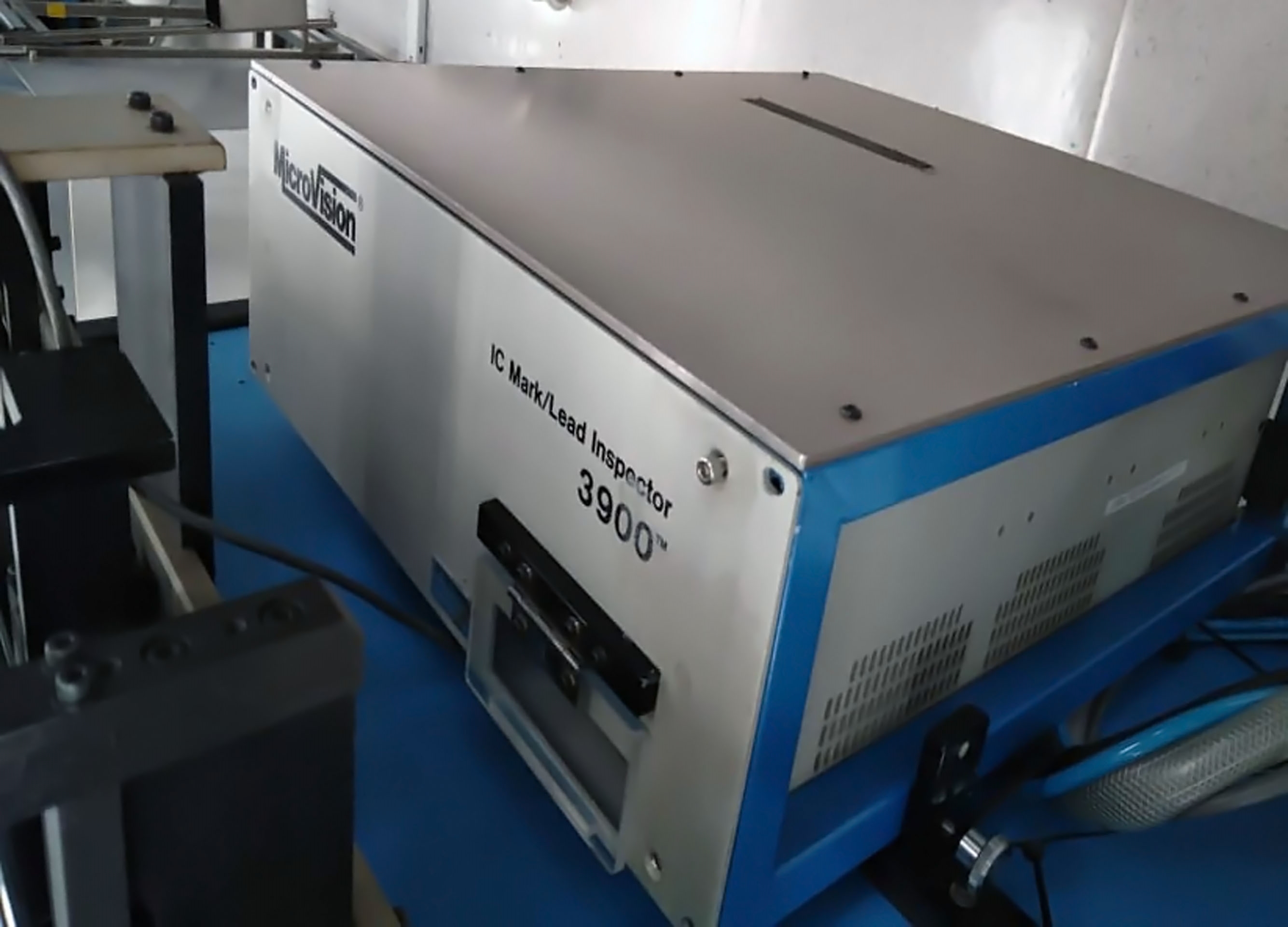
Used ESI / MICROVISION 3900 #9255783 for sale
URL successfully copied!
Tap to zoom


ESI / MICROVISION 3900 is an innovative mask and wafer inspection equipment designed for advanced semiconductor device manufacturers. The system is comprised of two components: a digital high-resolution imaging microscope and an automated image analysis platform. The microscope component of ESI 3900 is equipped with advanced optics including a unique 5x zoom lens that allows for the capture of extremely detailed images of even the smallest mask or wafer features. A solid-state CCD camera, advanced digital signal processing circuitry, and an integrated electronic control unit complete the microscope setup. Additionally, the microscope stage is designed to accommodate any size or shape of substrate, making it extremely versatile. The image analysis platform of MICROVISION 3900 is powered by a powerful proprietary algorithm designed to automatically detect and document any defects in the captured digital images. This algorithm is supplemented with a user interface that allows for greater control over the analysis process. The results of the analysis can be displayed in a variety of ways such as an ADC image format for quick visual assessment, or a more detailed CSV or XML format for more in-depth analysis. In addition to its mask and wafer inspection capabilities, 3900 also features several other advanced functions. Its enhanced image stitching functionality allows for the generation of high-resolution images at broad field of views. The machine also features a high-speed particle and crystal counting mode ensures that crystal phonology defects can be identified and documented quickly and accurately. ESI / MICROVISION 3900 is ideal for semiconductor device manufacturers who require advanced, high-precision mask and wafer inspection capabilities. Its powerful image analysis algorithms, user-friendly interface, and versatile construction make it an ideal choice for modern industrial labs.
There are no reviews yet

