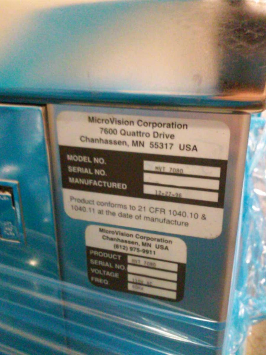
Used ESI / MICROVISION MVT 7080 #9187367 for sale
URL successfully copied!
Tap to zoom


ESI / MICROVISION MVT 7080 Mask & Wafer Inspection Equipment is a sophisticated imaging and analysis system designed to provide reliable and accurate inspection of masks and wafers. It combines advanced optical imaging technology and advanced image processing algorithms to identify potential defect locations on mask and wafer surfaces. ESI MVT 7080 features an optical measurement unit composed of a precision interferometer, chromatic aberration corrector and 10x/0.4 objective lens for high-accuracy imaging. The aberration corrector ensures that accurate scanning and imaging capabilities are maintained even when working with large substrates or when the objective can't be perfectly aligned. An integrated 3-axis stage provides the ability to move the objective lens and sample around, allowing for the inspection of various sizes of masks and wafers. The imaging machine of MICROVISION MVT 7080 utilizes a high-resolution CCD line scan camera to capture and store images. The CCD camera has a 2048 pixel x 656 line resolution, and is capable of storing up to 128,000 pixels of data. Integration and analysis of data captured by the imaging tool is done through an embedded processing unit. The unit features algorithms for defect detection, inspection and judgement, as well as for other pattern processing tasks. It is capable of classifying defects in four categories: line width, open/short, missing and reflectivity. MVT 7080 also features a user-friendly control asset, providing users with an intuitive interface for all aspects of operation. This includes model functions, data entry, display adjustments, parameter settings and inspection results. An extensive range of additional features including statistical analysis and graphing capabilities further complement ESI / MICROVISION MVT 7080's capabilities. In summary, ESI MVT 7080 is an easy to use, reliable and accurate inspection equipment that provides users with comprehensive imaging and analysis capabilities. Its combination of advanced optics, imaging, and processing capabilities allows it to consistently and accurately identify potential defects on mask and wafer surfaces.
There are no reviews yet