Used HENNECKE HE-SIM-02 #9233425 for sale
URL successfully copied!
Tap to zoom



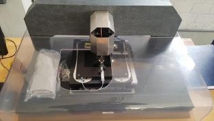

ID: 9233425
Semi-automatic measuring system
For sapphire wafer
Thickness range: 200 - 1500 μm
Square size substrates:
100 x 50mm: 20,4 sec
130 x 70mm: 28,2 sec
Part range:
Diameter, 2": < 51.5 mm
Diameter, 4": < 102 mm
Diameter, 6": < 153 mm
Stages: X,Y (High-precision)
(2) Chromatic confocal sensors
Sensor speed: 200 mm / sec (Standard)
Sensor frequency: 4.000 Hz (Standard)
Meander pitch: 5mm (Standard)
Sample size: 160 mm (Maximum)
Thickness, TTV, LTV, sori, bow and warp:
X,Y Stage resolution: X, Y = 5 μm
Sensor type: Chromatic confocal
Sensor resolution: Z = 60 nm
Dynamic range (Sensor): 2000 μm (Each side)
Accuracy thickness: 200 nm
Precision thickness: ± 200 nm
Precision TTV: ± 300 nm
Accuracy sori, bow, warp: 300 nm
Precision sori, bow, warp: ± 300 nm
Roughness values:
Saw mark: 1 mm Width (Maximum)
Waviness: 4 mm Width (Maximum)
Saw mark and roughness (Ra and Rz):
X, Y Stage resolution: X,Y = 5 μm
Sensor type: Chromatic confocal
Sensor resolution: Z = 60 nm
Dynamic range (Sensor): 2000 μm (Each side)
Precision saw mark: ±1200 nm
Accuracy saw mark: 300 nm
Precision roughness 0.8 μm (Ra and Rz): ±3 %
Accuracy roughness (Ra and Rz): 30 nm
Central processing unit:
Operating system: Windows 7
User interface: (17) Displays
Power supply: 230 V, 16 A, 1.5 kW.
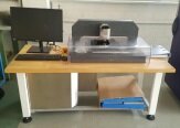
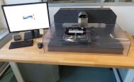
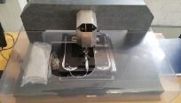
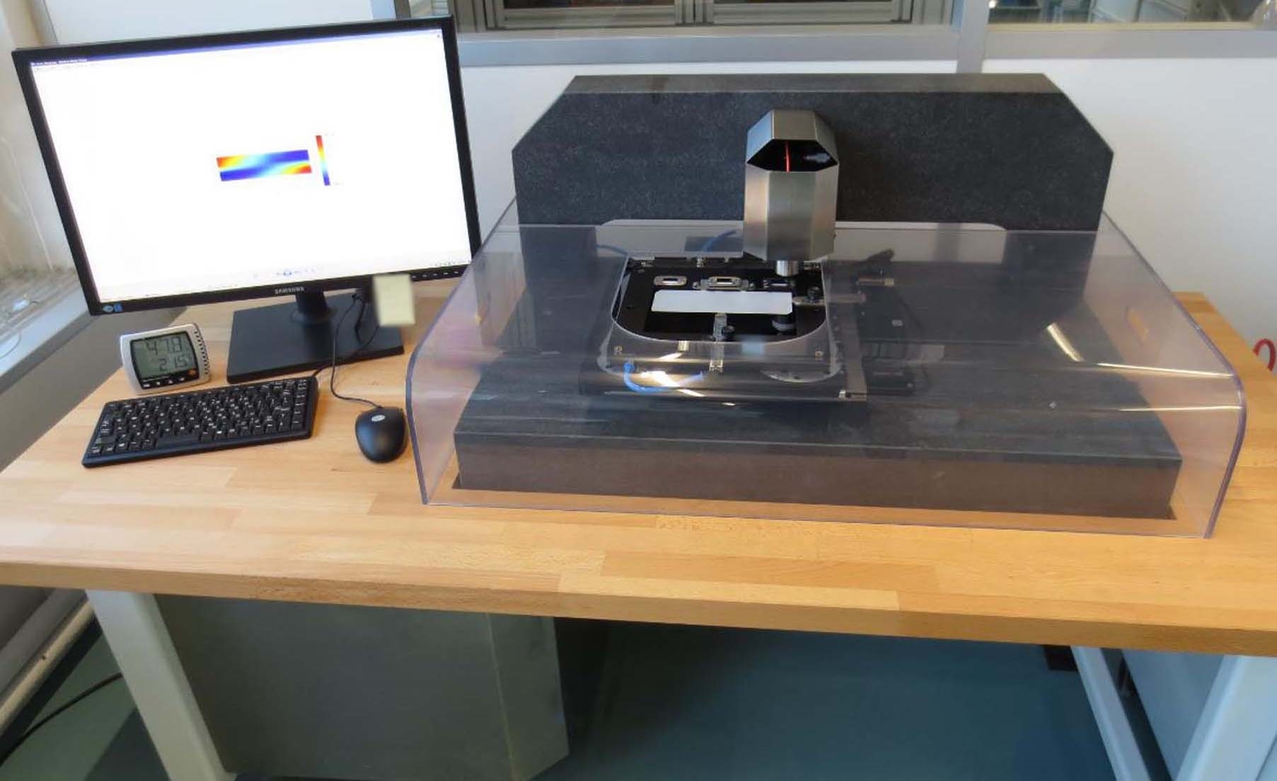
HENNECKE HE-SIM-02 mask & wafer inspection equipment is a reliable and precise optical inspection system, designed to detect defects in wafers and masks used in the manufacture of semiconductors. The instrument is capable of inspecting up to 12" wafers at resolutions up to 0.5µm, providing extremely sensitive and accurate results. HE-SIM-02 consists of an inspection unit which is mounted on a XYZ motion stage. The unit is capable of freely moving the inspection heads over the wafer and can detect a wide variety of features and defects with maximum accuracy. The machine is equipped with an advanced sensing unit that can detect up to 2,000 pixels with a single scan, allowing it to rapidly scan and detect defects across the entire wafer surface. The tool combines an innovative array of sensors and LED lights, providing superior inspection performance. It is capable of detecting misshaped patterns with precision, as well as a variety of defects and irregularities such as broken wires, damaged vias, foreign particles etc. The asset is designed to process data in real-time for quick and accurate results. It is also designed to be resistant to environmental and temperature changes, ensuring reliable performance in a variety of conditions. HENNECKE HE-SIM-02 also provides advanced software capabilities which can process data in real-time, allowing engineers to adjust and optimize their inspection strategies. The software also features automated reporting capabilities, providing users with detailed feedback on the state of their wafer or mask. This information can help manufacturers improve their processes and production yields. In conclusion, HE-SIM-02 is an advanced and reliable inspection model for wafers and masks. Its advanced hardware and software capabilities provide users with unmatched accuracy, allowing manufacturers to rapidly detect and identify defects with no compromise in performance.
There are no reviews yet
