Used HERMES MICROVISION / HMI Epointer #9259976 for sale
URL successfully copied!
Tap to zoom









ID: 9259976
Wafer Size: 12"
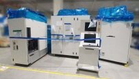
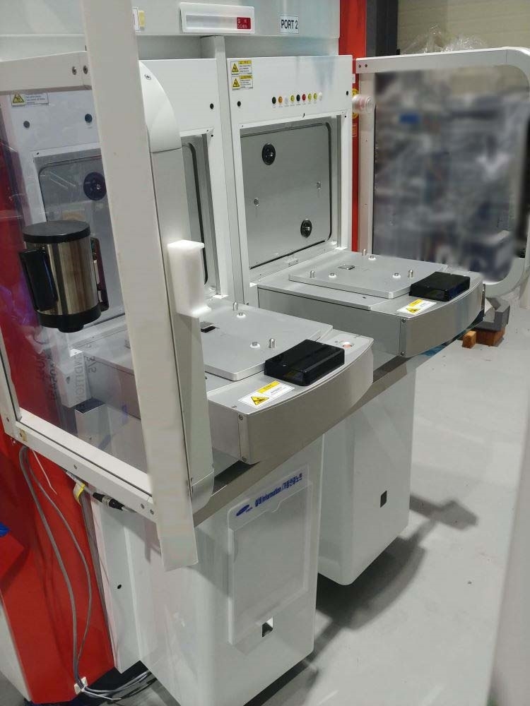
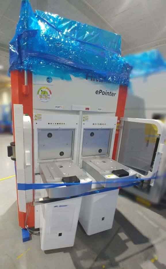
E-Beam inspection system, 12", parts machine
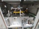
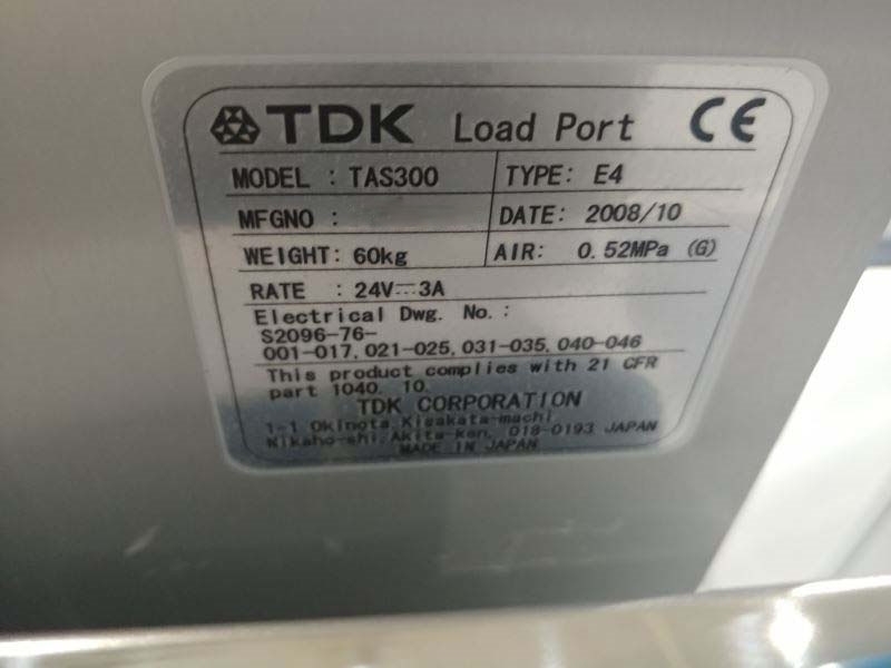
(2) TDK E4 Loaders
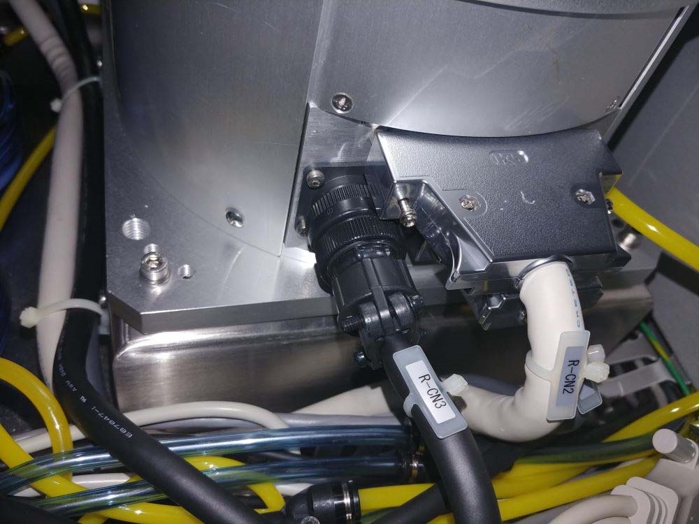
RORZE RR716 ATM Robot.
HERMES MICROVISION / HMI Epointer is a mask and wafer inspection equipment designed for use in photolithography and nano-lithography fabrication processes. It is used to accurately and reliably inspect high resolution masks and wafers for errors and defects. HMI Epointer system has a low-coherence light source and a digital CCD/CMOS camera. This allows it to capture high-contrast and sharp images of defects, even at the nanometer scale. The inspection unit uses a powerful optical comparator, which is capable of montaging images of different masks and wafers to compare their features against one another. This ensures defect detection across all areas of the substrate, regardless of its scale or structure. HERMES MICROVISION Epointer machine also has a built-in automated defect review capability. This cuts down on the need for manual intervention, reducing inspection time and boosting efficiency. It can easily detect errors like missing images or line width errors with its powerful automation tool. This inspection asset is also designed to be easy to use and operate. It is highly ergonomic, allowing the user to adjust the position of the microscope to best suit their needs. It also has an intuitive user interface, with settings that can easily be adjusted to match specific inspection requirements. Epointer model supports both SEMI-E82 and SEMI-E87 standards. This makes it suitable for use in a variety of photolithography and nano-lithography applications. Its image processing technology allows for accurate and high-quality detection of defects and errors. The results are displayed in multiple display modes, featuring both 2D and 3D images. Overall, HERMES MICROVISION / HMI Epointer makes mask and wafer inspection easier and more accurate than ever before. Its advanced features and ergonomic design make it perfect for use in a variety of photolithography and nano-lithography applications.
There are no reviews yet
