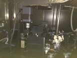
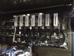
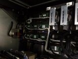
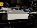
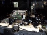
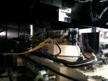
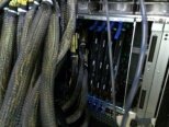
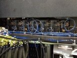
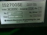
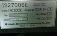
Used HITACHI IS 2700SE #9123256 for sale
URL successfully copied!
Tap to zoom



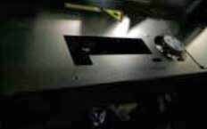

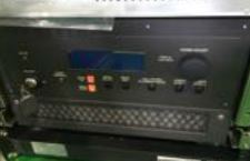

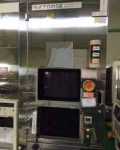

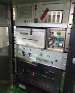




























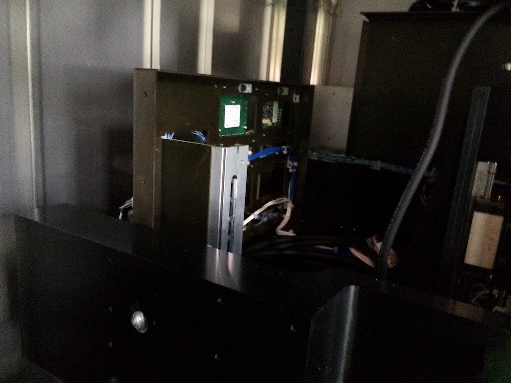

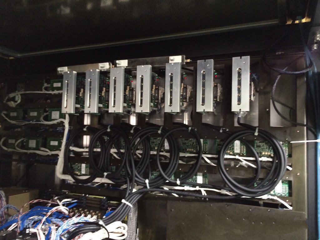

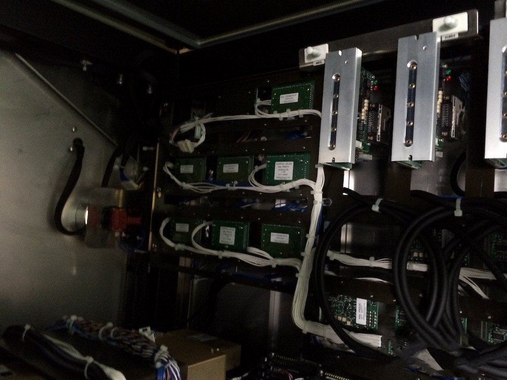

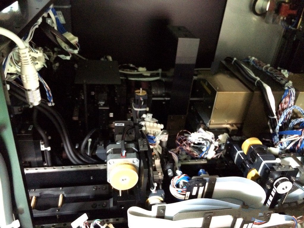







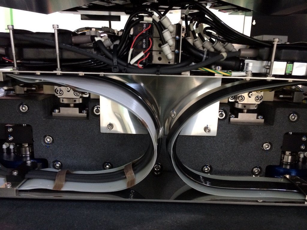

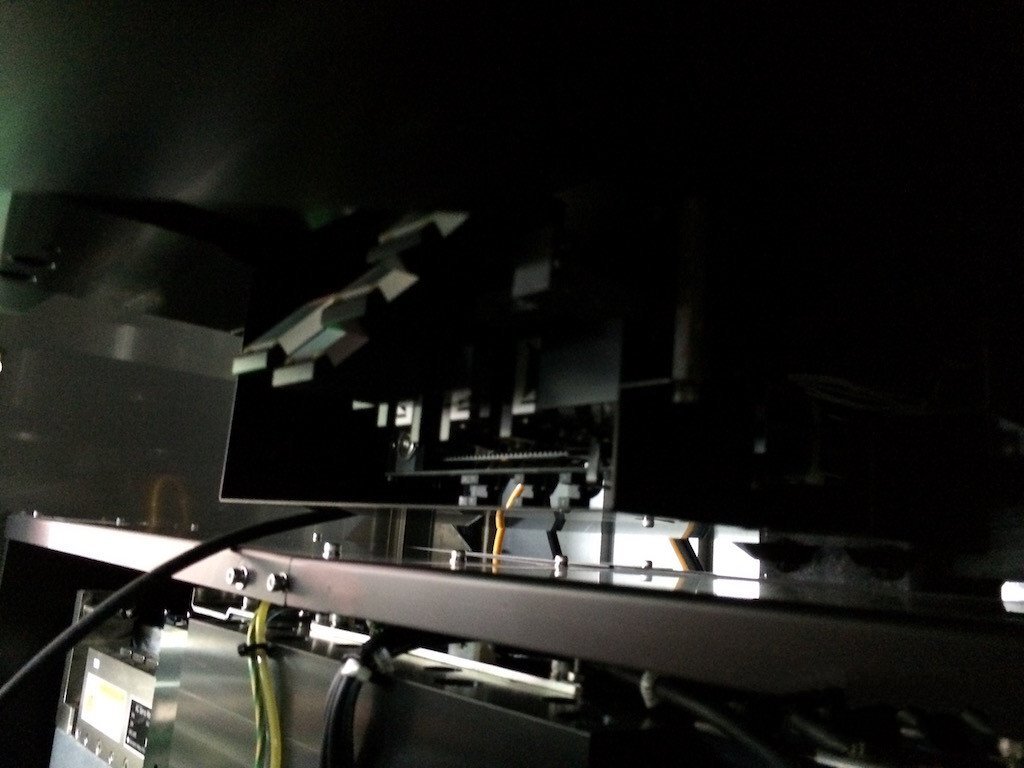


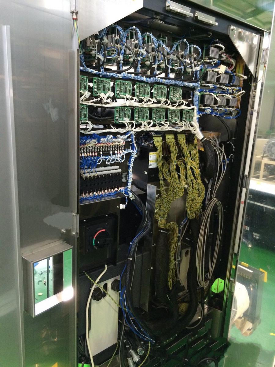

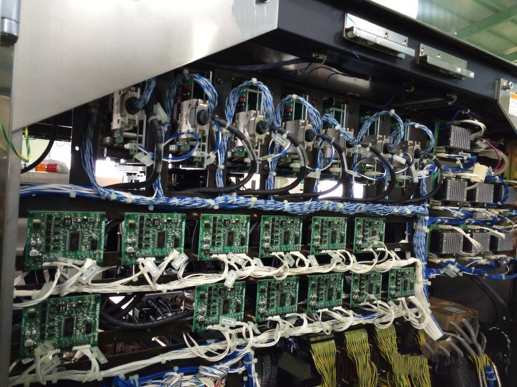


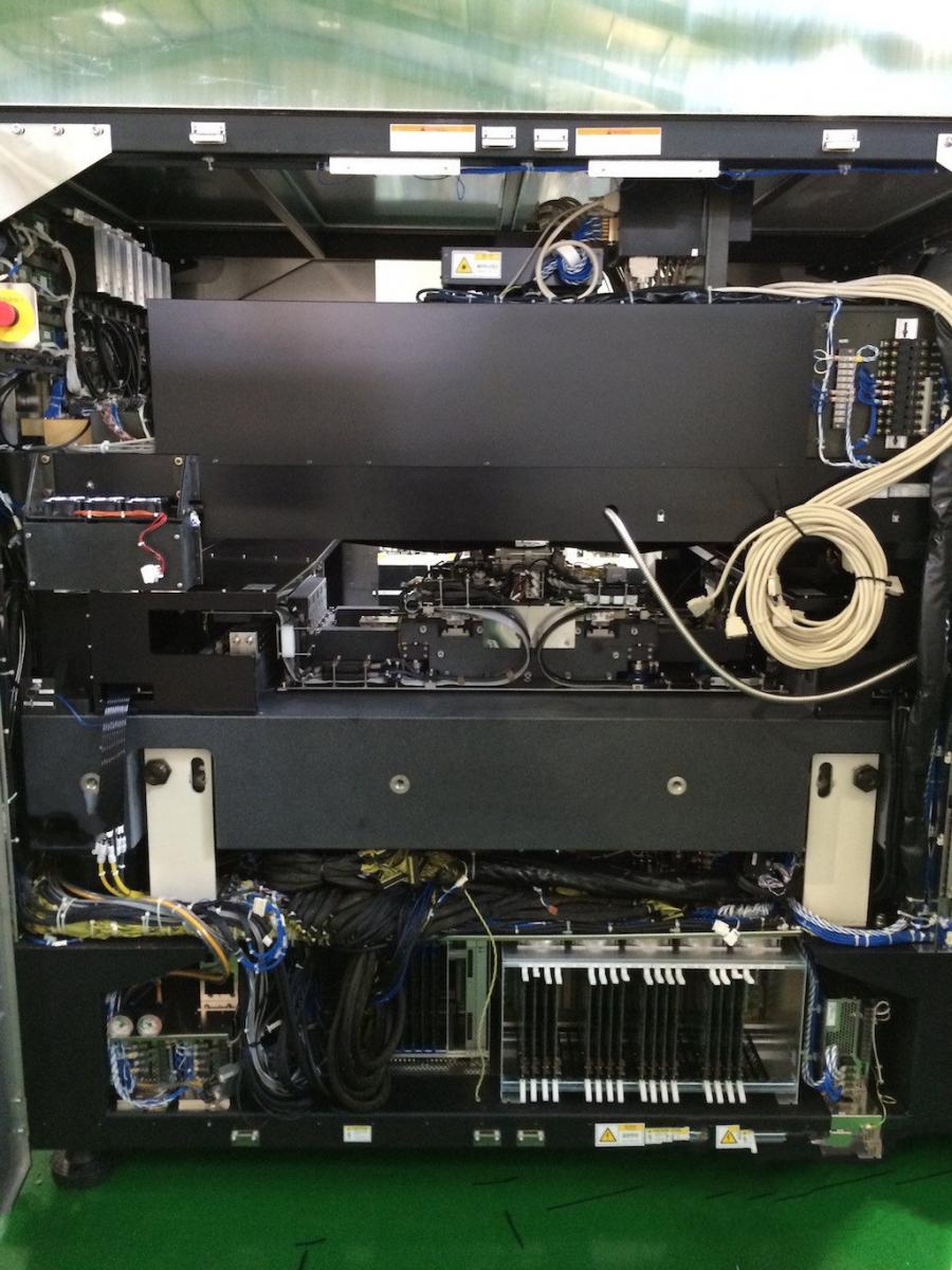

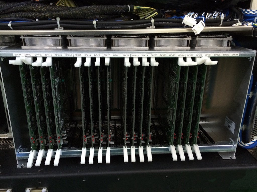

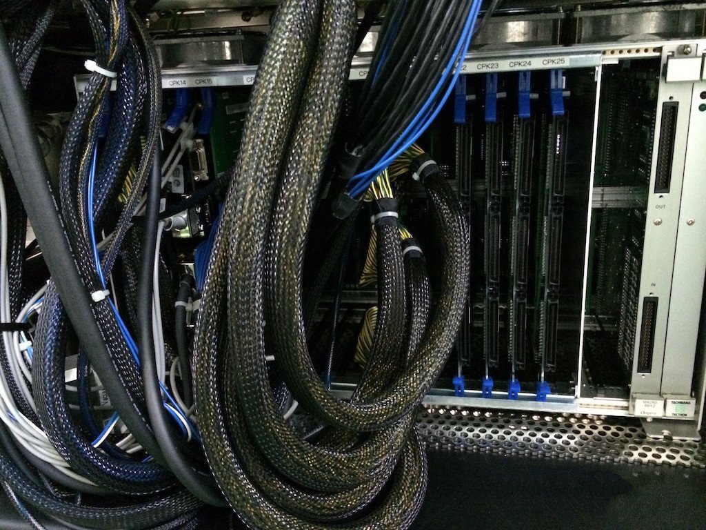

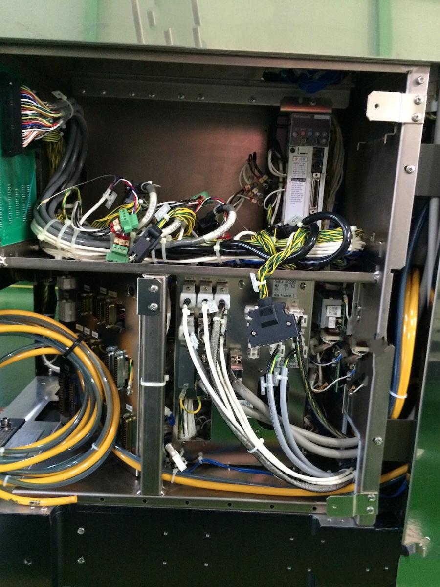







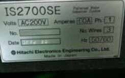

ID: 9123256
Wafer Size: 12"
Vintage: 2004
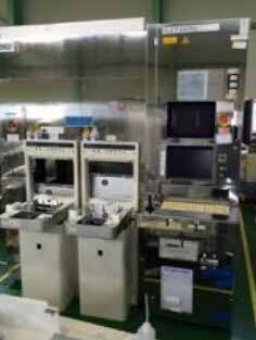
Defect inspection system, 12"
Process: Scanning electron microscope(SEM)
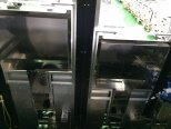
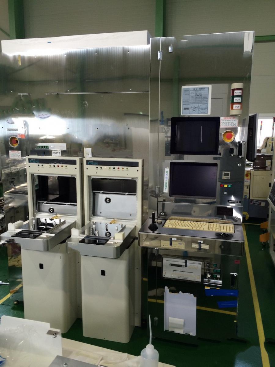
(2) Loadports: TDS TAS3000
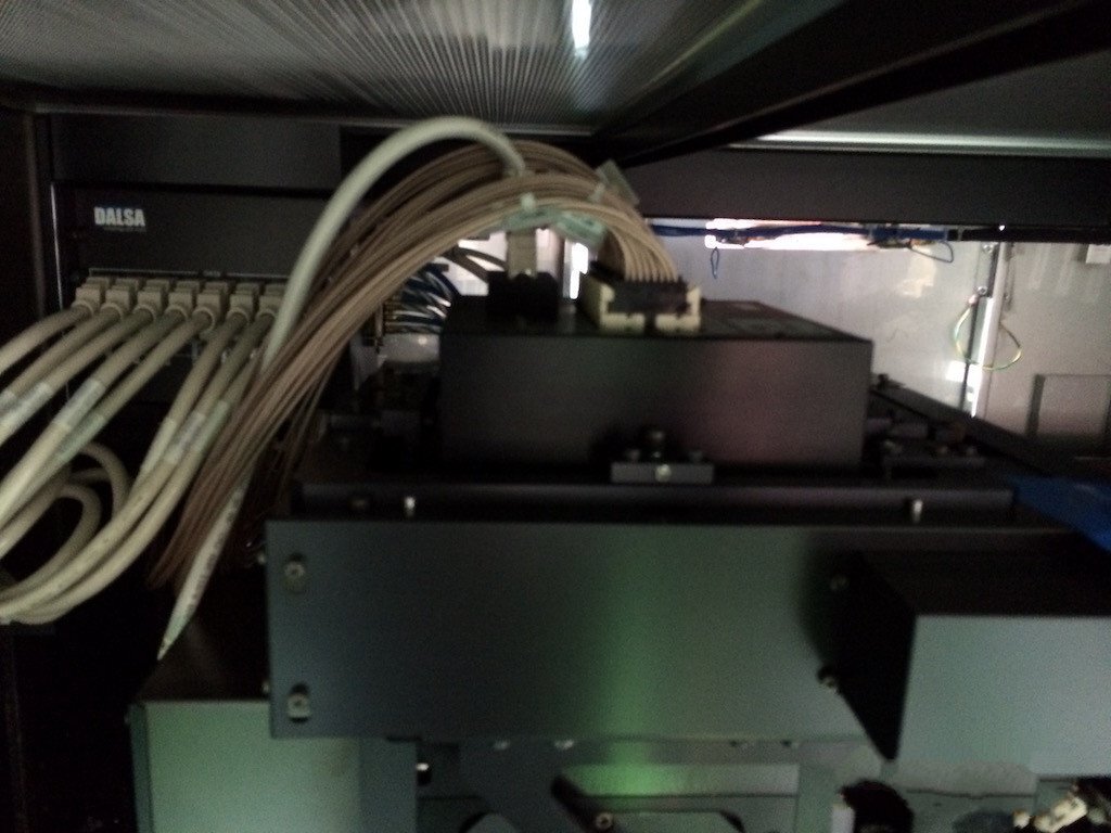
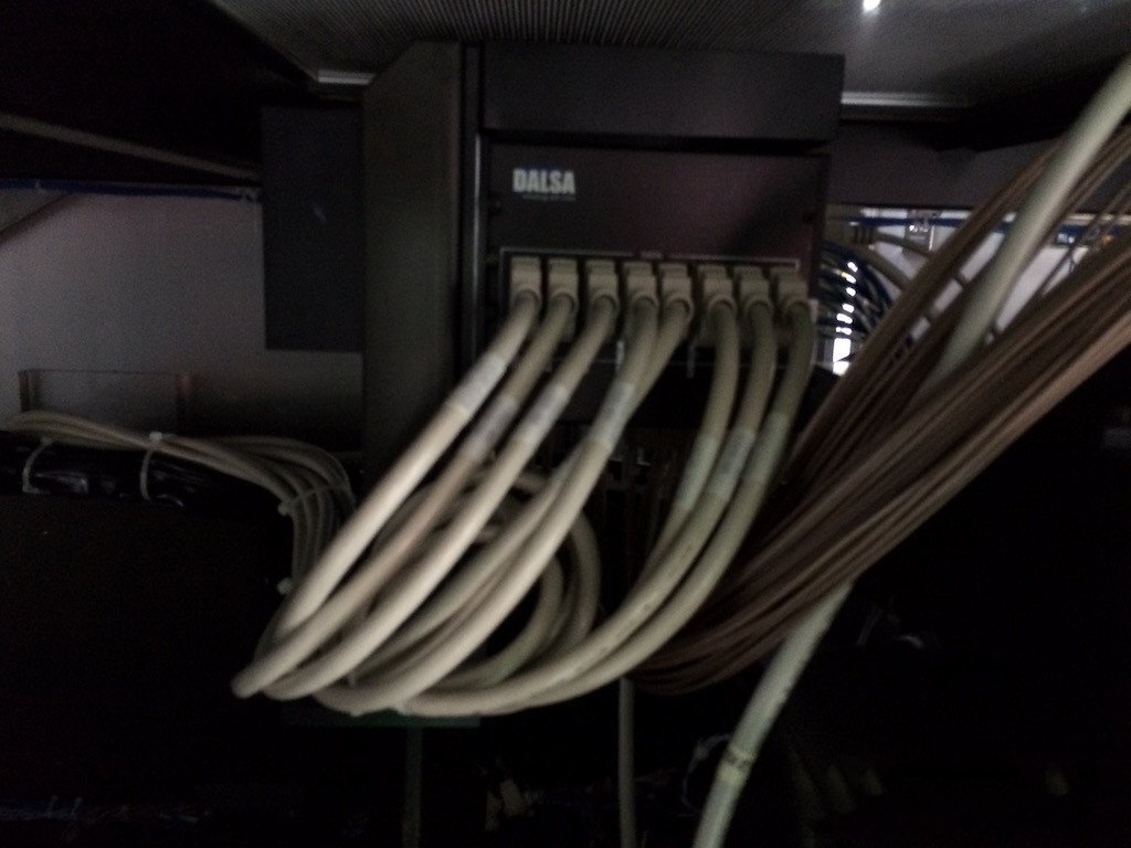
Dalsa controller
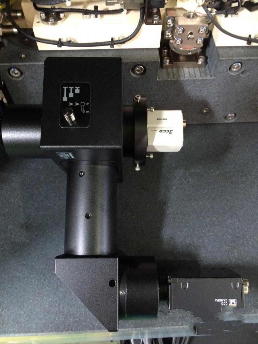
TDI Sensor
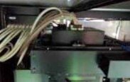
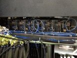
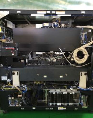
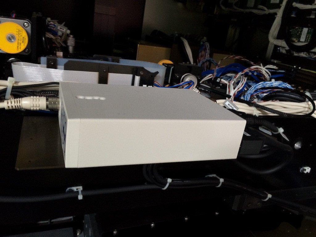
Laser box
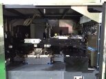
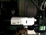
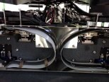
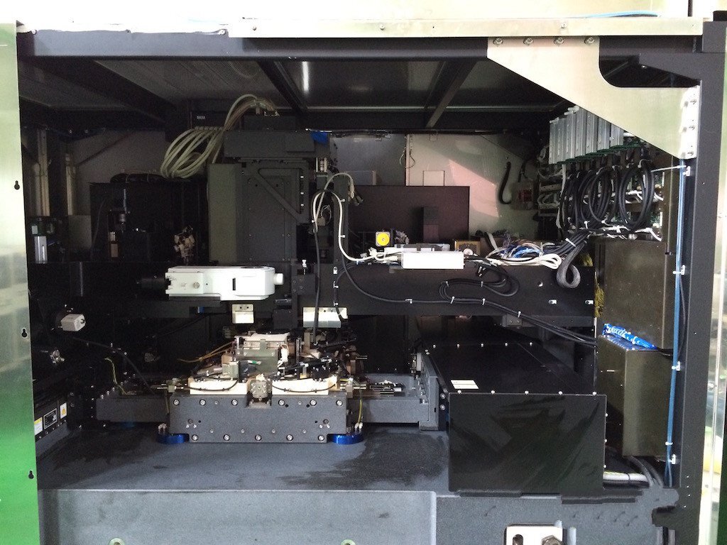
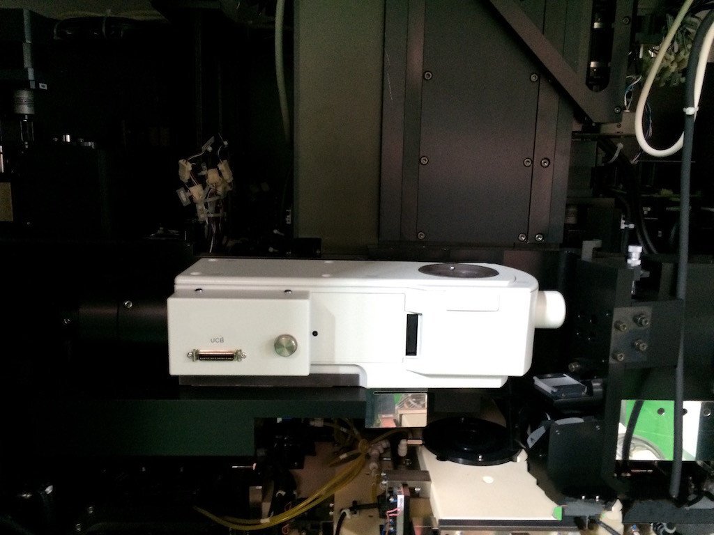
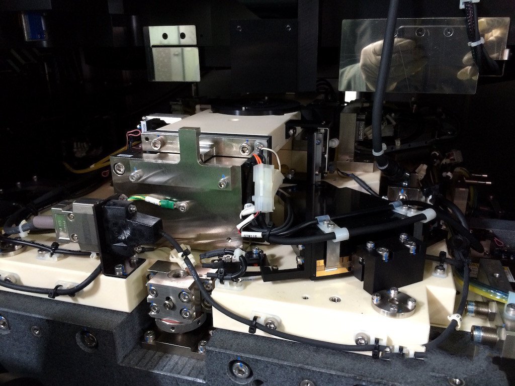
Microscope
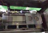
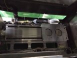
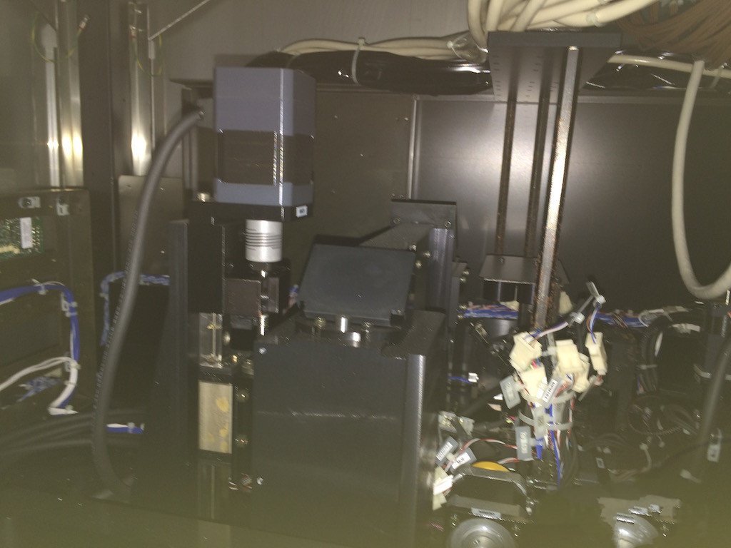
Stage assy
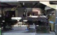
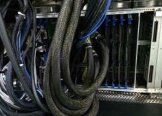
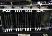
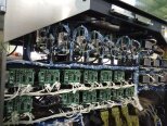
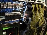
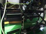
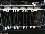
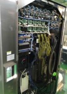
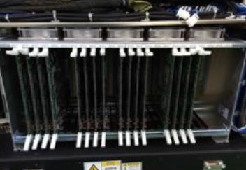
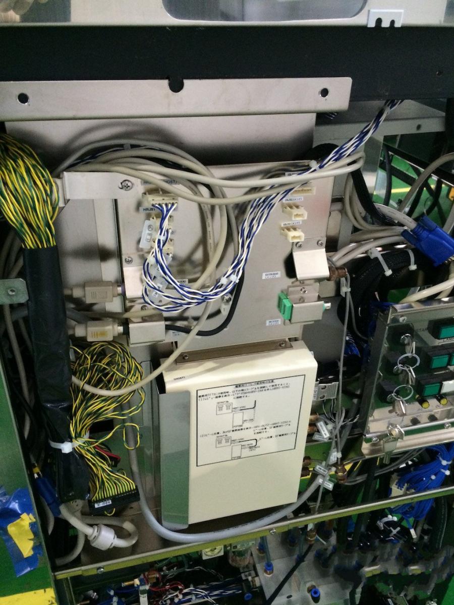
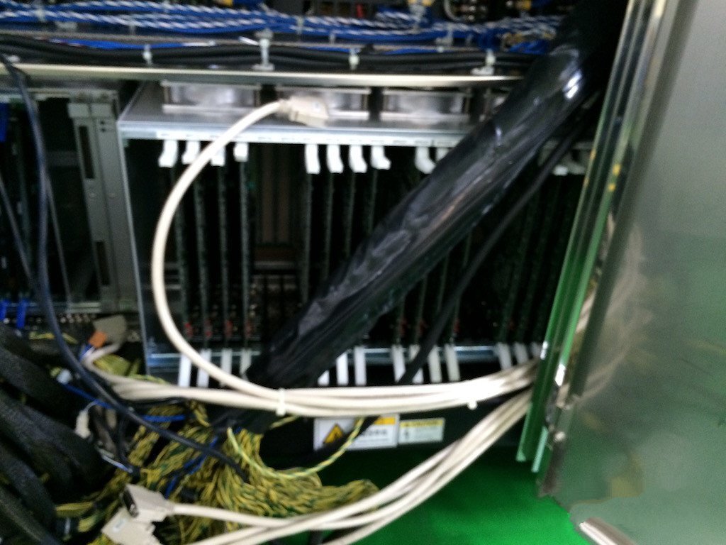
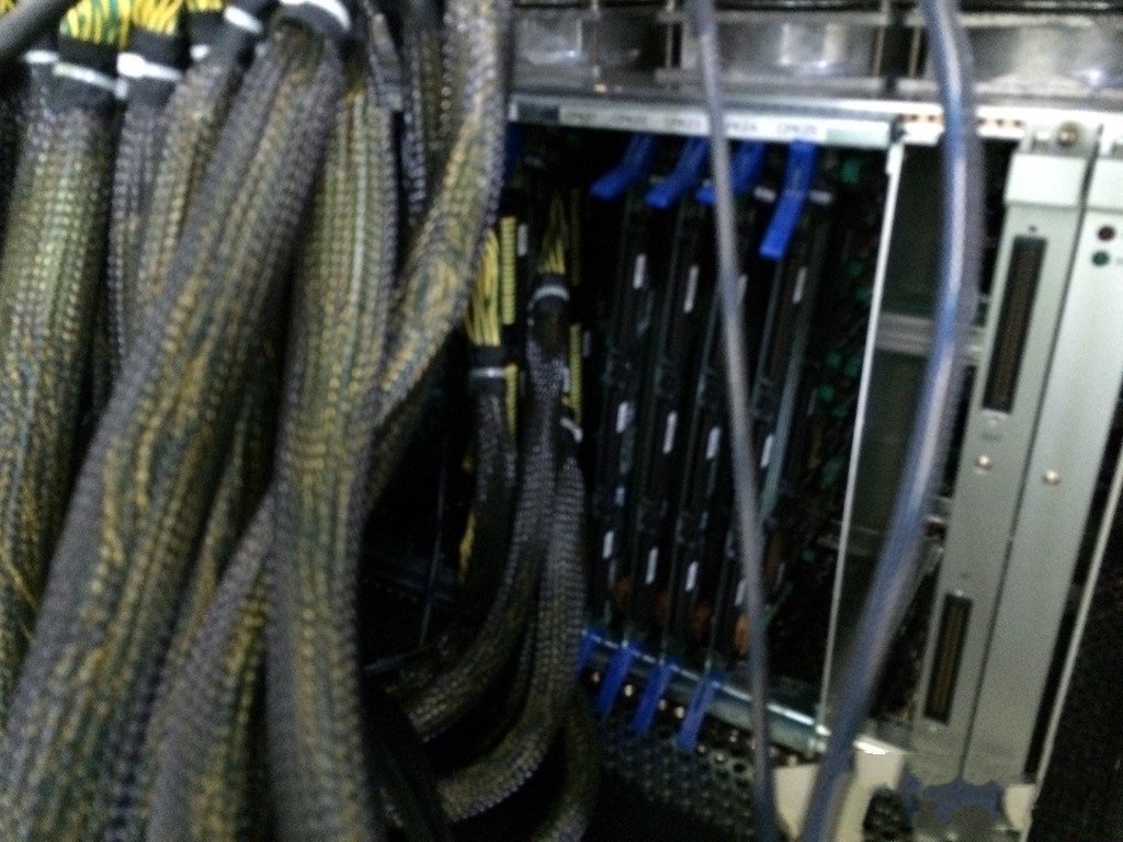
Controller card cage (left):
CPK B/D Slot 11~15, 20, 22~25
CPK B/D Slot 16~19, 21
Macro 6642 B/D
TECTRON B/D
Controller card cage (right):
BPK B/D Slot 11~14,17~20, 22~25, 28~31
BPK B/D Slot 15,16, 21,26,27, 32~34
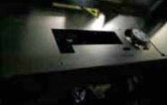
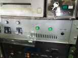
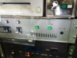
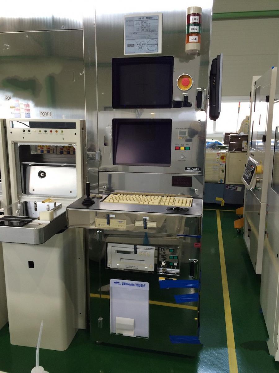
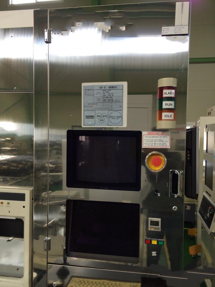
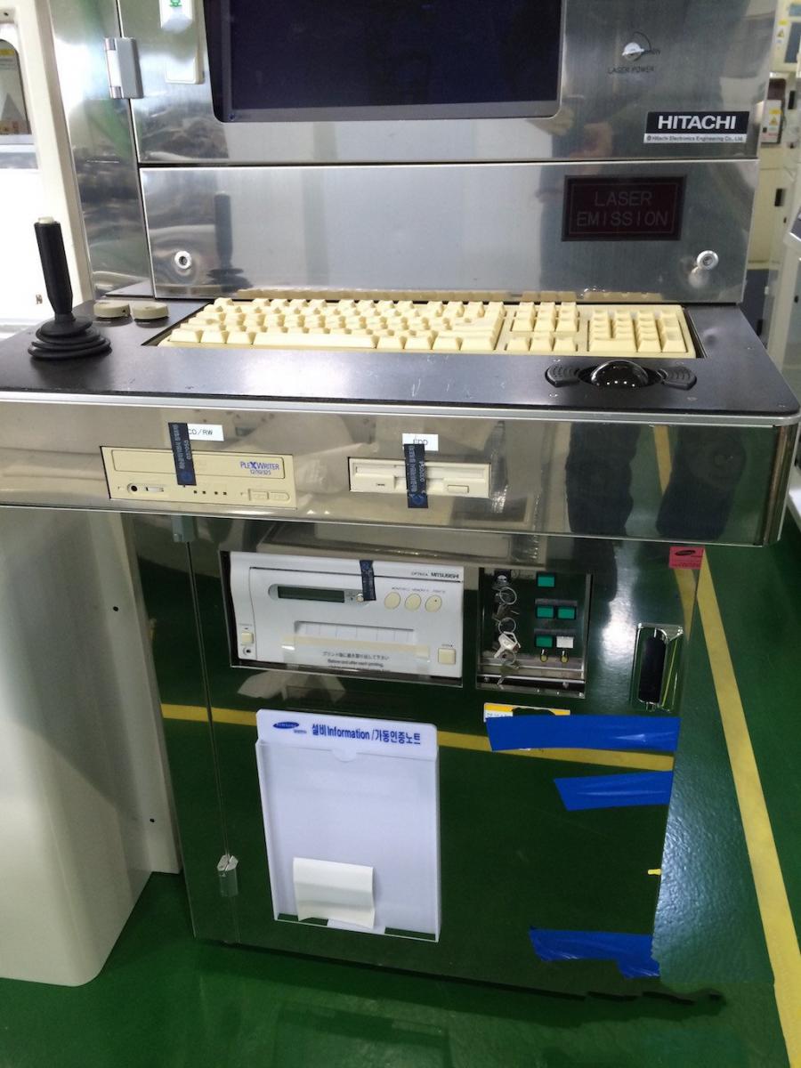
Operation module:
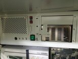
System computer
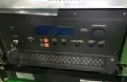
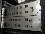
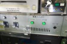
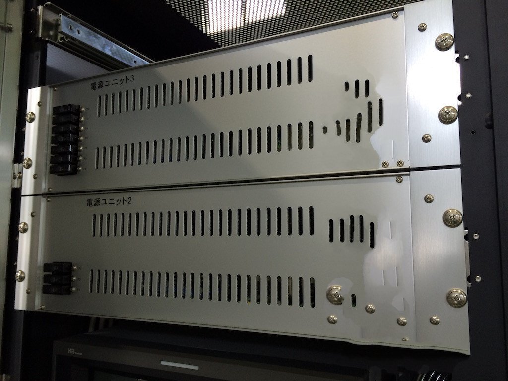
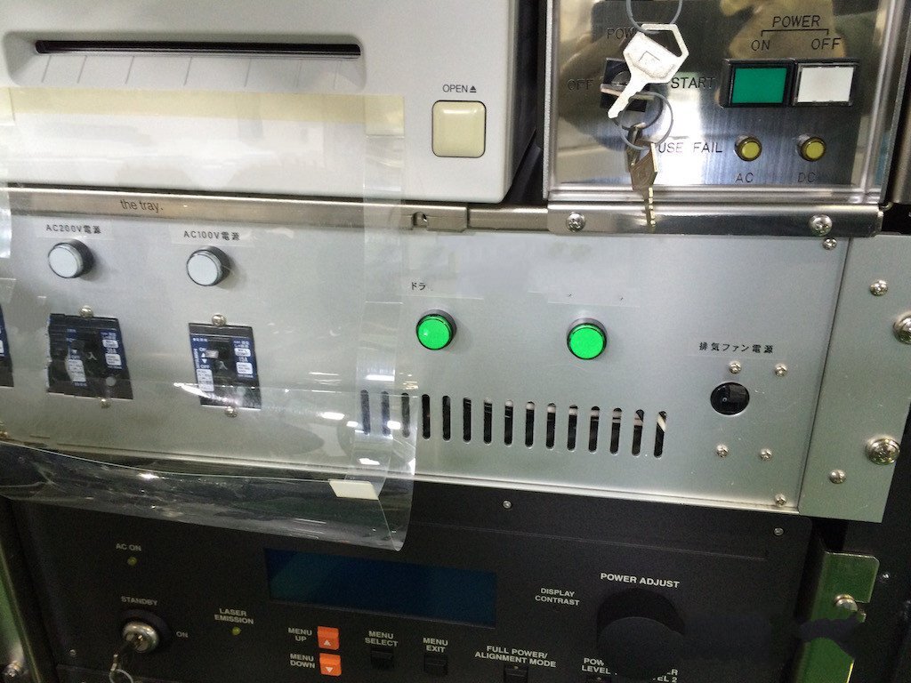
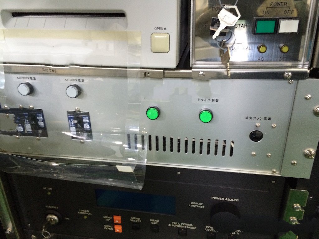
(3) Power supplies
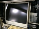
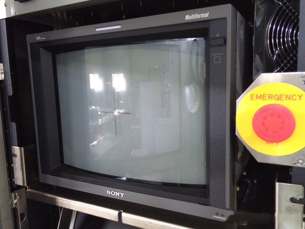
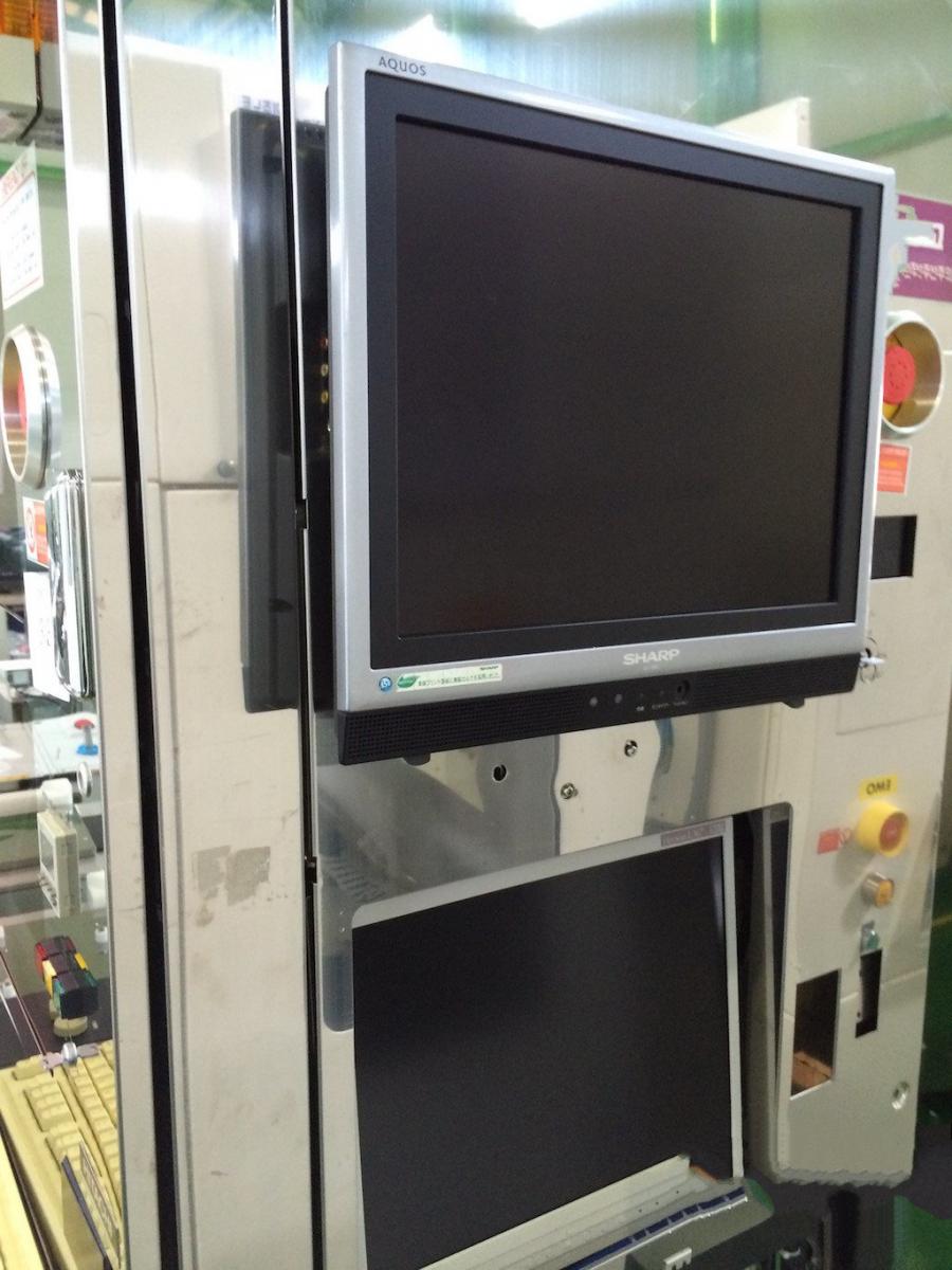
CCD monitor
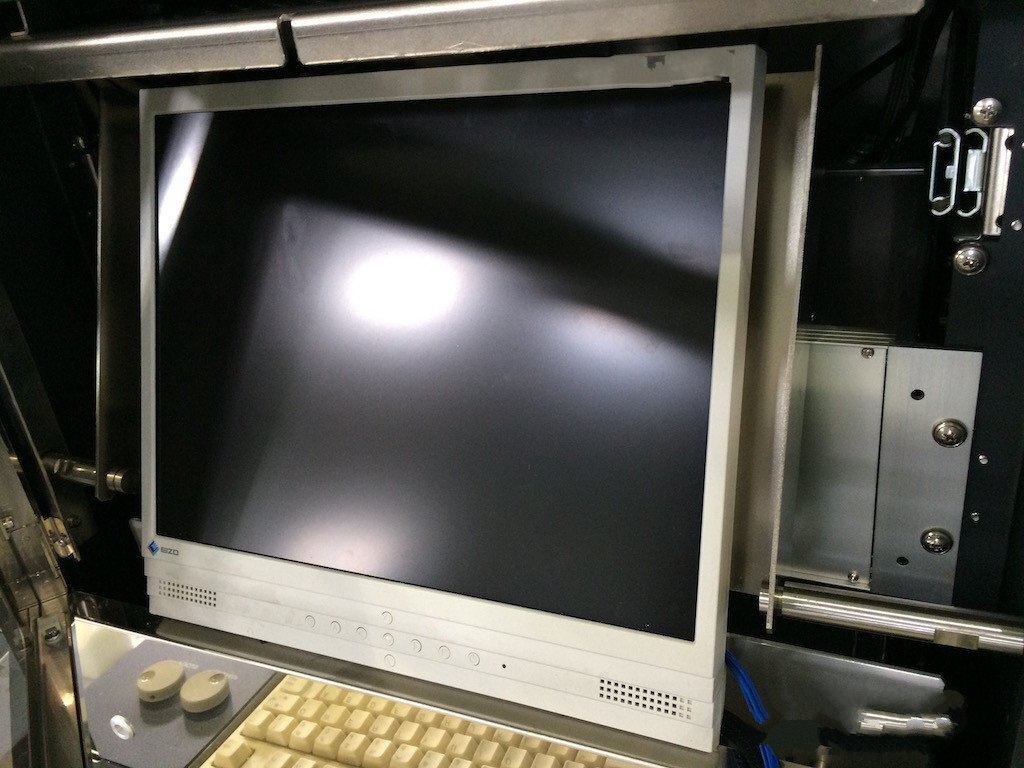
PC monitor
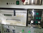
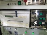
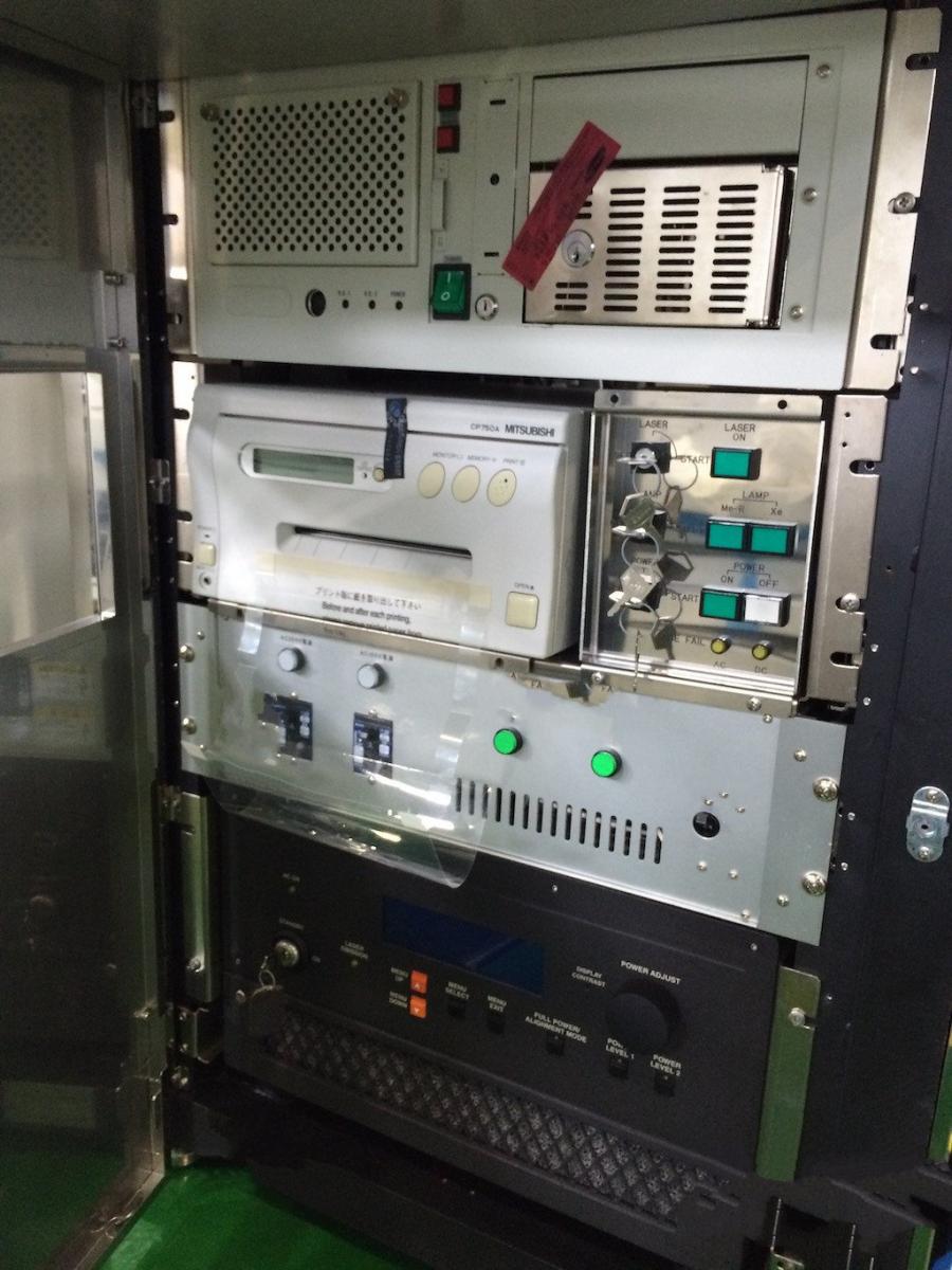
Video printer
Laser power switch box
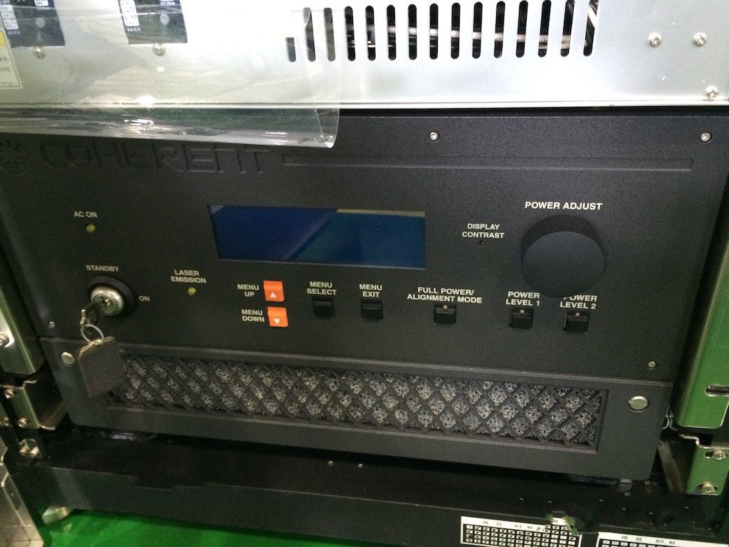
Coherent laser controller
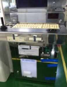
Keyboard, joystick, trackball
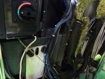
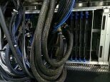
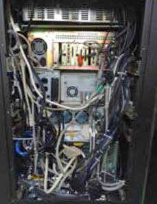
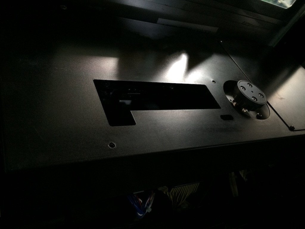
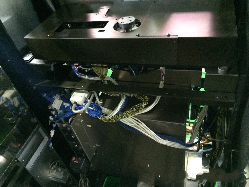
Rear cover missing
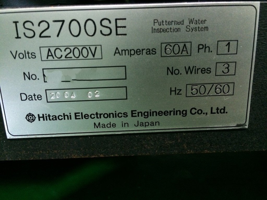
Power: AC200V, 1 Phase, 3-wires, 50/60Hz, 60A
2004 vintage.
HITACHI IS 2700SE mask & wafer inspection equipment is an advanced automated optical inspection system designed for the efficient analysis of photomasks and wafers in the semiconductor and electronics manufacturing industry. It provides high-speed and remarkably accurate inspection capabilities that enable the rapid identification of defects in both new and existing designs. The design of IS 2700SE features a precision, 6-axis robot and an 80-megapixel image processing sensor that can inspect both early-stage masks and wafers with extremely fine detail. It offers both front-side and reverse-side as well as complex multiple-side inspections. In addition, its wafer inspection capabilities include identifying defects on quartz and glass substrates. HITACHI IS 2700SE utilizes high-precision optical imaging technologies to accurately detect even the smallest defects with up to 2 nanometers in size. Unique to the unit is the multi-beam confocal optics configuration which allows the machine to obtain a substantially more accurate image than a typical lens tool can. This enables IS 2700SE to identify defects more swiftly, registering accurate results in a matter of seconds. With an array of probes available to handle any combination of mask and wafer types, the asset can inspect flat surface, microelectrode, step surfaces, as well as grooved materials. The model has a range of automated tests and can be used with a variety of software that allows users to view the results and set the parameters of the tests so they can be conducted more quickly and efficiently. The software includes defect classification, detection adjustment, area-oriented inspection, fault-localization, threshold patterns, and sequential defect maps. HITACHI IS 2700SE offers a wide range of tools that allow users to customize how the tasks are performed. These include image and defect memory, automatic transform programming, and detection workflow monitoring. It also has a user-friendly GUI interface that simplifies operation and eliminates the need for an operator to be present. IS 2700SE is a highly reliable and efficient tool for the efficient analysis and automated detection of defects in photomasks and wafers. With its automated tests and user-friendly GUI, it offers powerful inspection capabilities and is a must have for any semiconductor and electronics manufacturing facility.
There are no reviews yet

