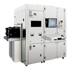
Used HITACHI LS-6700 #9087166 for sale
URL successfully copied!
Tap to zoom


ID: 9087166
Particle inspection system
Throughput: Under normal inspection mode 37 WPH
Particle detection size: 0.05um and higher
Wafer size: Configured for 12"
Includes manual
Currently in cleanroom.
HITACHI LS-6700 is a mask & wafer inspection equipment developed for the semiconductor industry. It is capable of accurately measuring defects down to the nanometer scale on both wafers and masks. The system consists of three modular parts - a light source unit, an optical scanning unit, and a computer unit. The light source unit emits a broad spectrum of light that is then directed via a beam splitter to the optical scanning unit. The optical scanning unit consists of a high-definition camera, lens, and a real-time position detection unit. Together, these components enable the mask & wafer inspection machine to capture high-resolution images of the wafer or mask surface with nanometer-level accuracy. The computer unit consists of a large memory capacity and powerful processing capacity, allowing it to process the imaging data quickly. It also includes an intuitive graphical user interface (GUI) that allows users to easily and quickly customize the masked & wafer inspection process. In addition to providing information on defect size and position, HITACHI LS 6700 also recognizes a variety of defect types. This includes measuring open/shorts, step heights, pits,and other surface imperfections down to the nanometer scale. Thanks to its internal algorithms, users of the mask & wafer inspection tool can quickly identify and flag potential defects. In terms of repeatability and accuracy, LS-6700 is one of the best systems on the market. It boasts an excellent repeatability of 0.9 percent, and a positioning accuracy of up to 0.2 nanometers. The asset is also well-suited for multi-die wafer inspection and is capable of analyzing up to four dies at once. Overall, LS 6700 is an excellentmask & wafer inspection model, capable of providing high-accuracy imaging with nanometer-level resolution. Its modular design makes it flexible and easy to use, while its powerful processing and repeatability capabilities allow for fast and accurate defect detection.
There are no reviews yet