Used HITACHI LS 9300A+ #293812143 for sale
URL successfully copied!
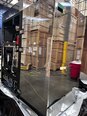
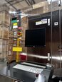


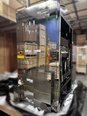
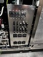
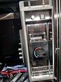
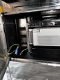
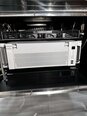
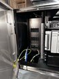
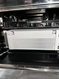
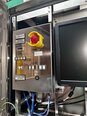
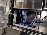
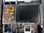








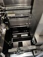

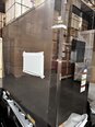
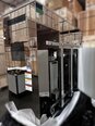
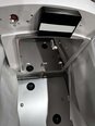



Tap to zoom
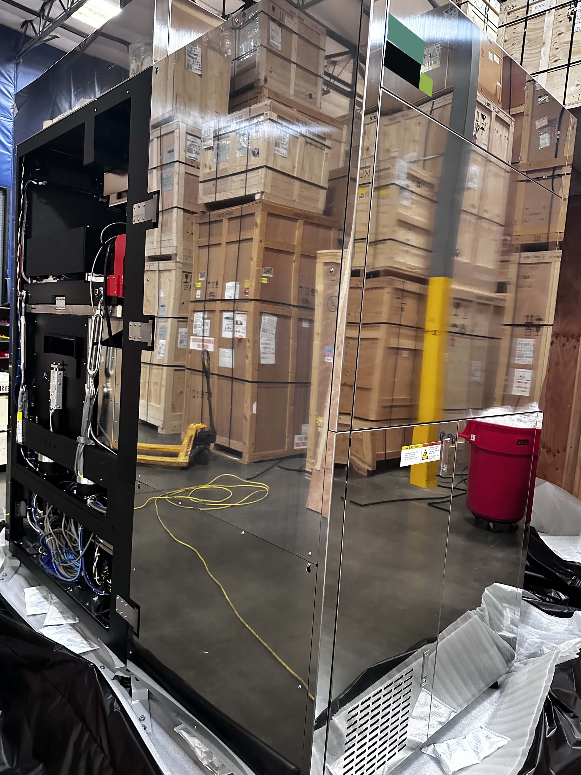

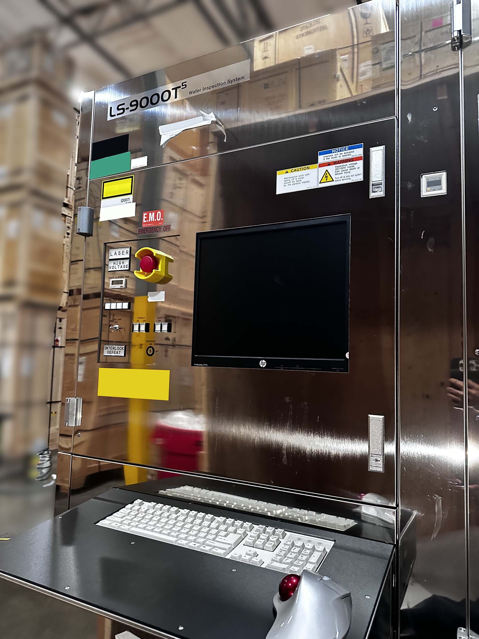
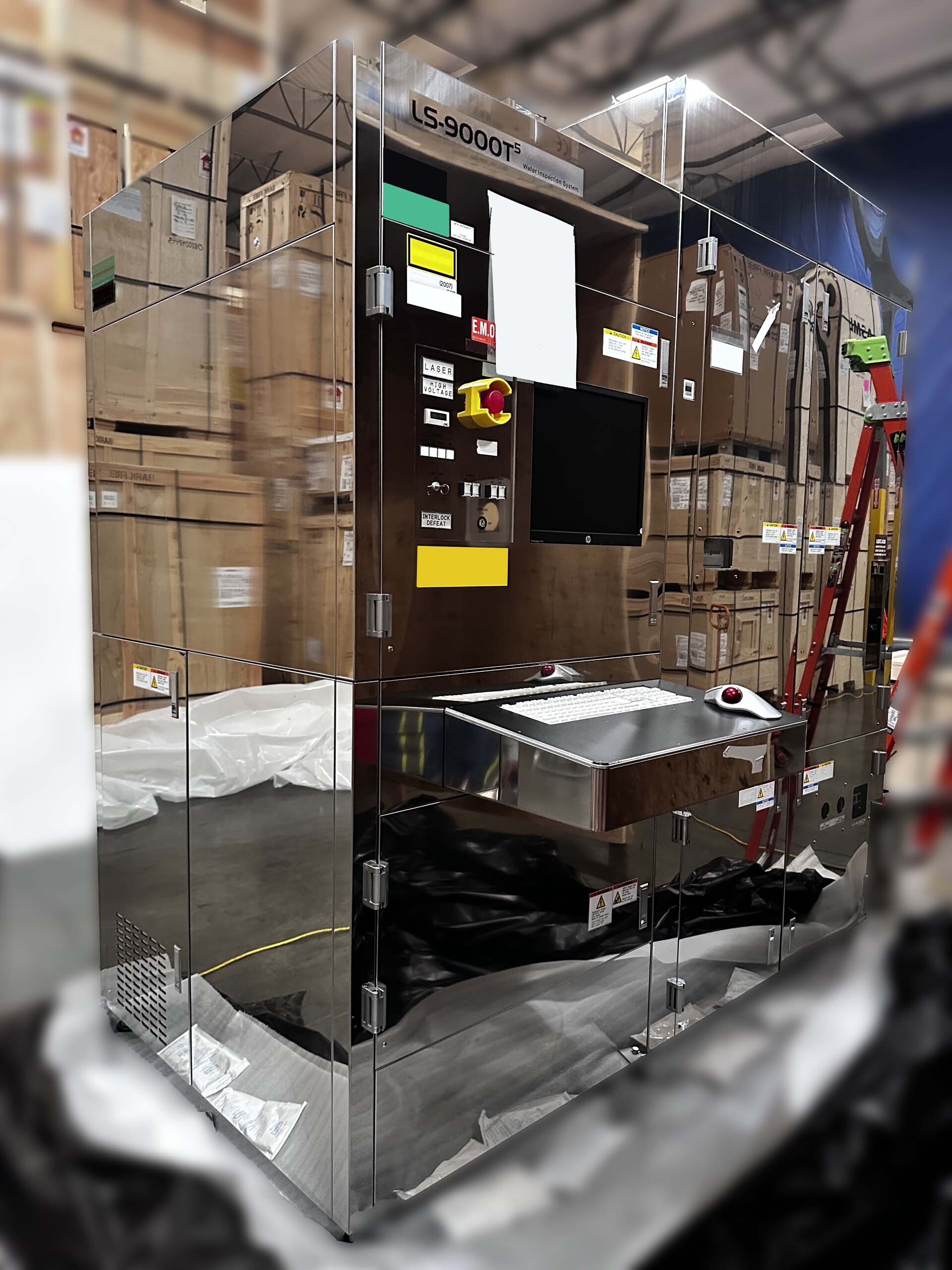
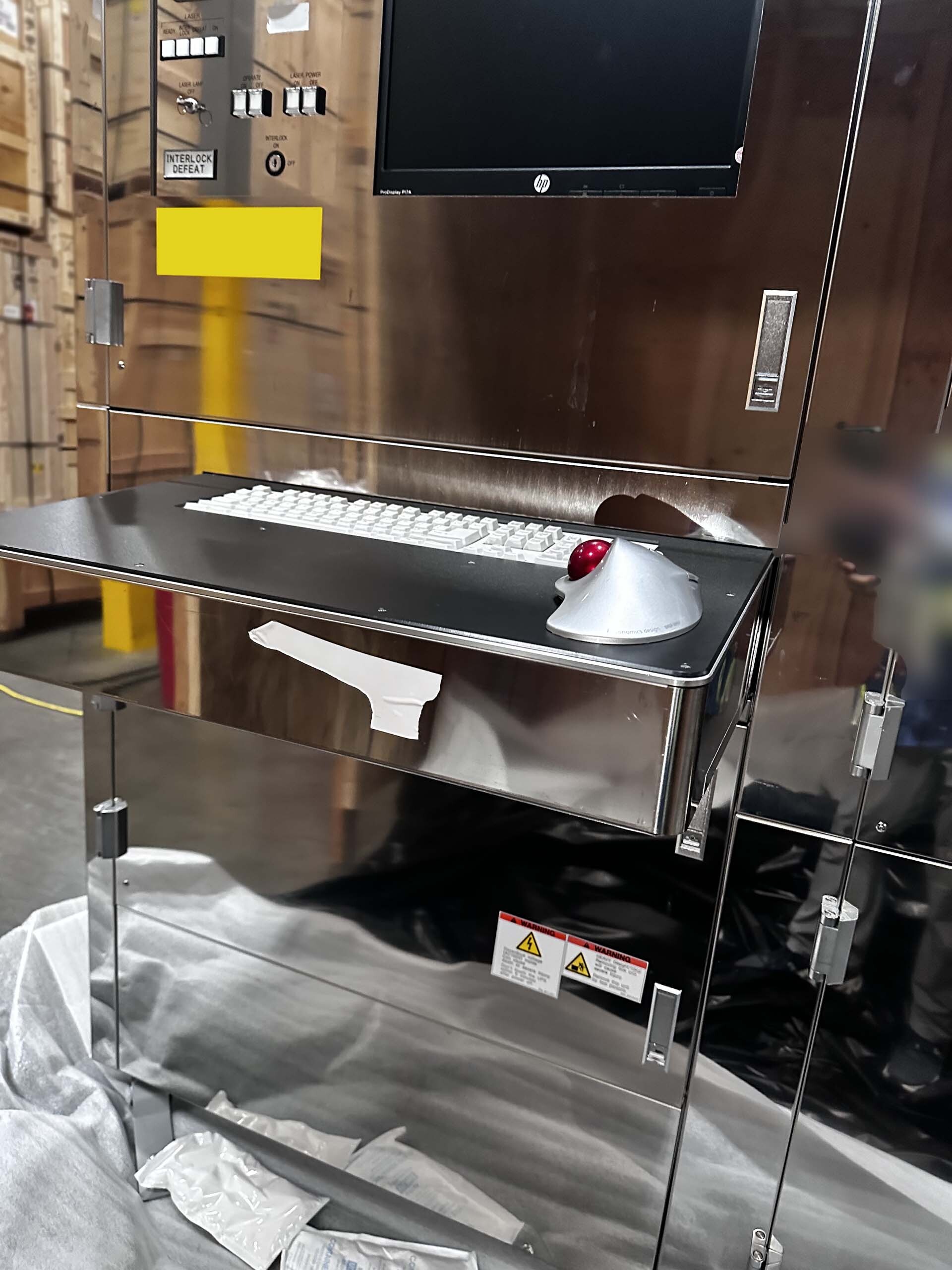
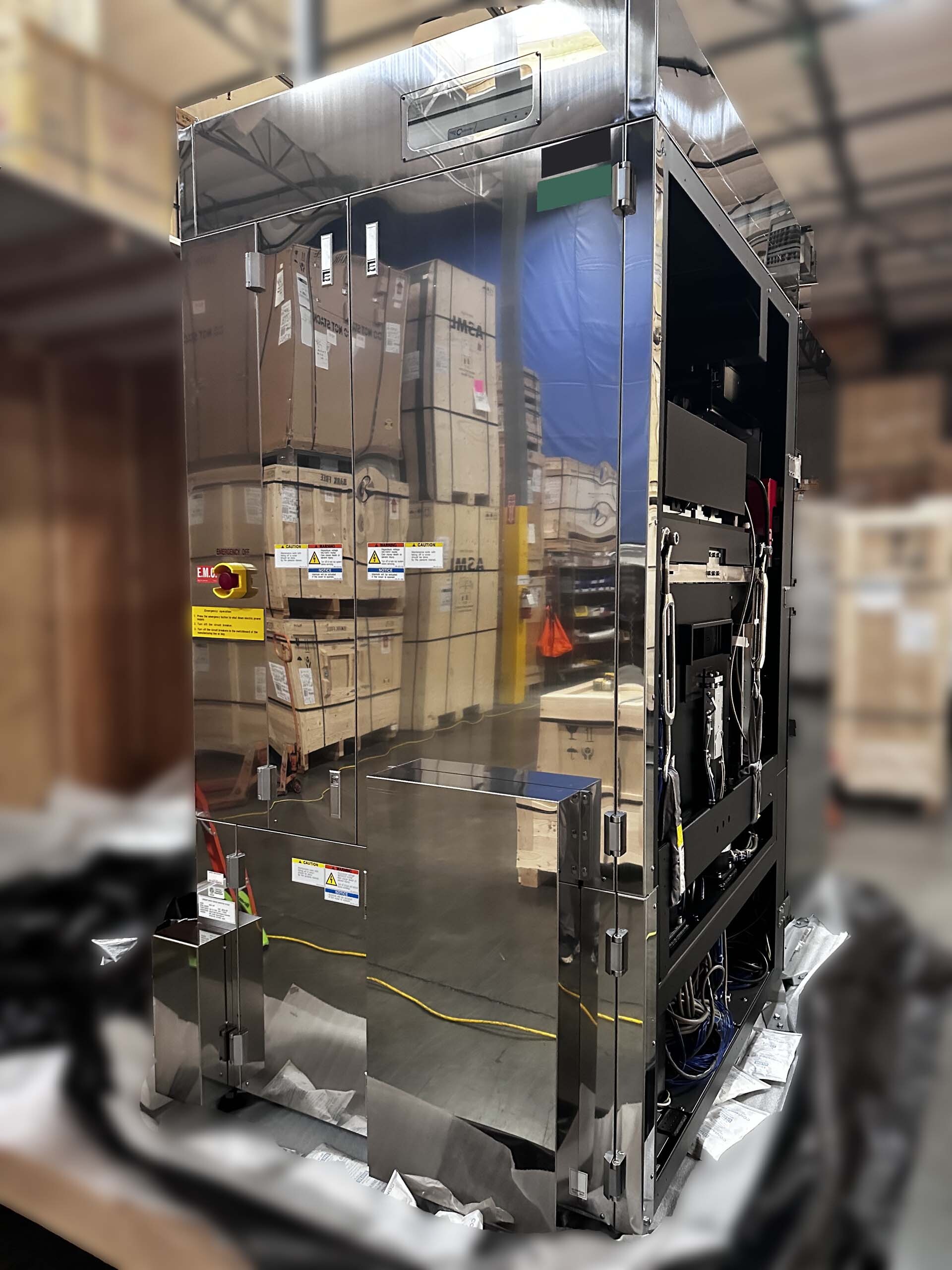
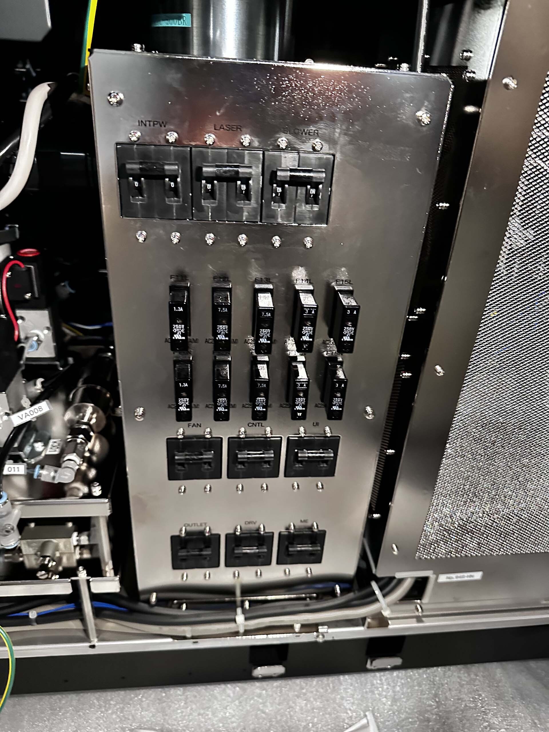
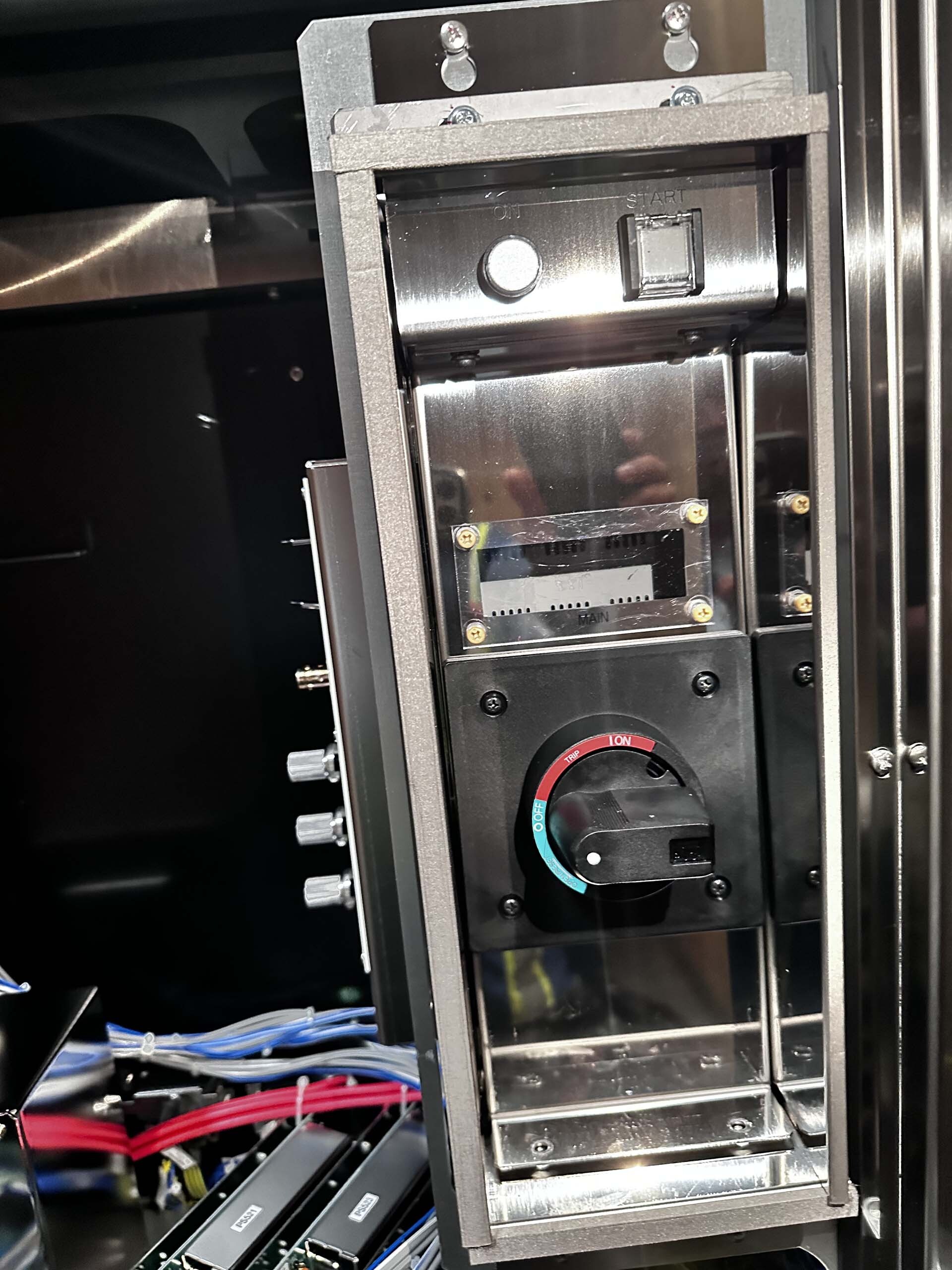
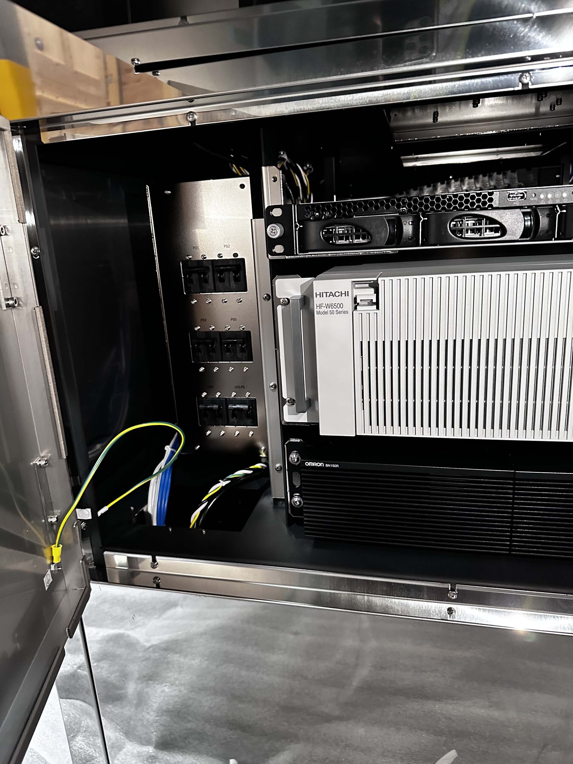
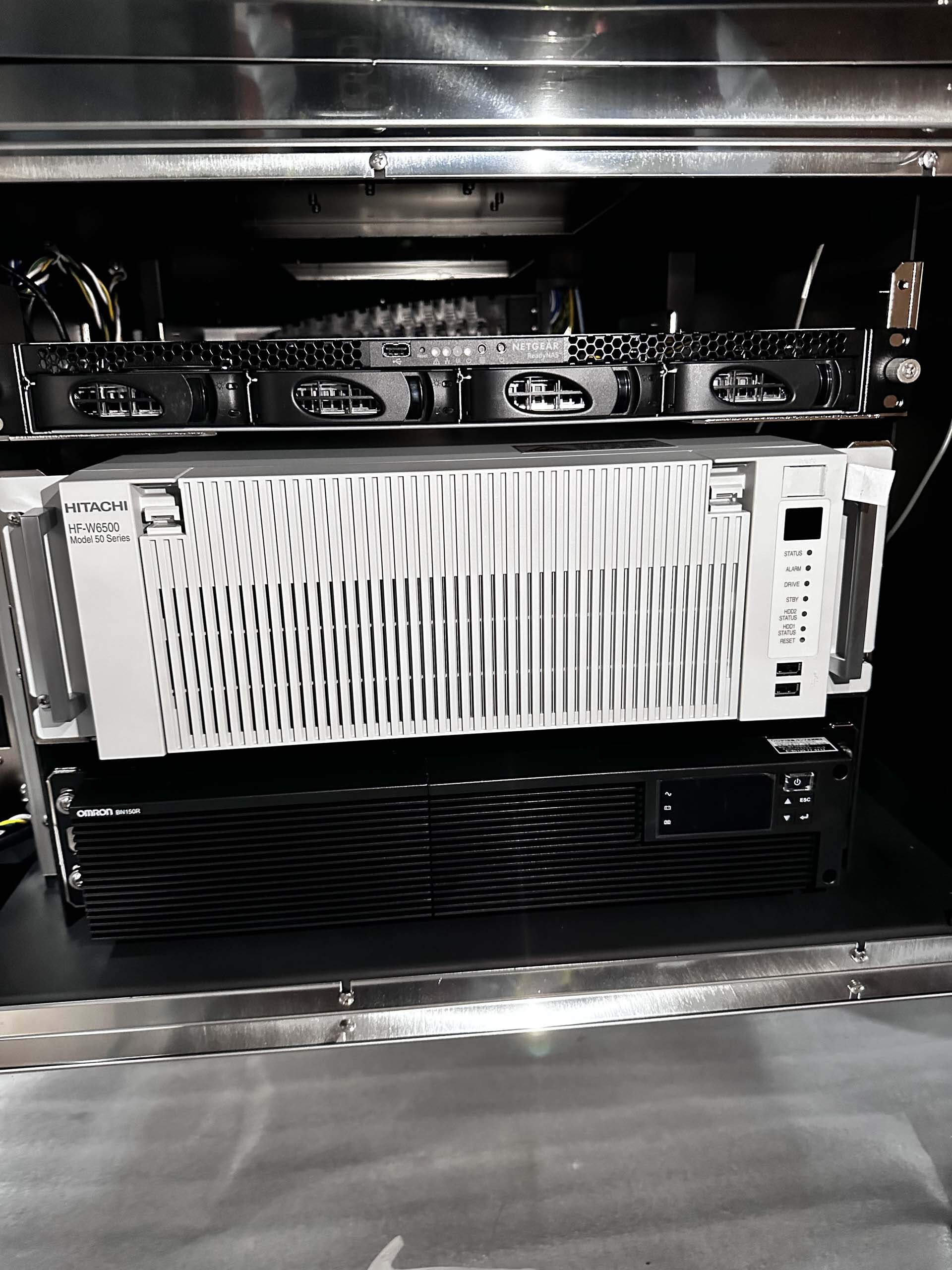
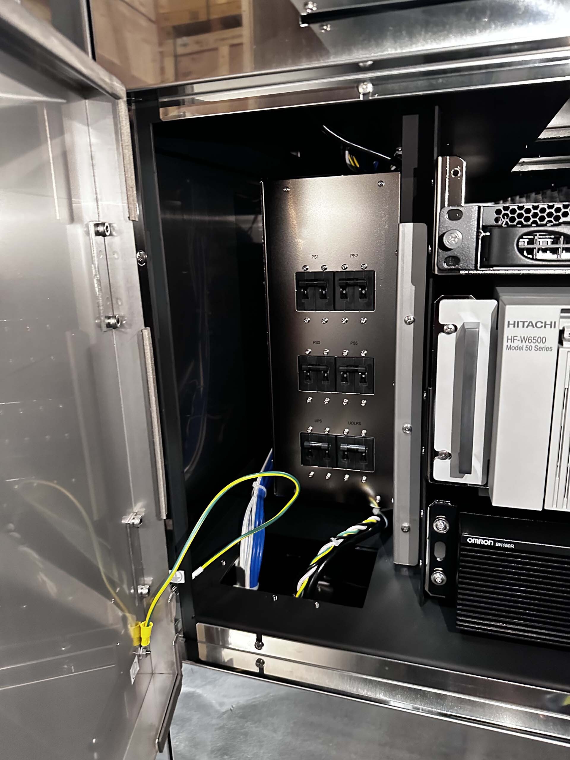
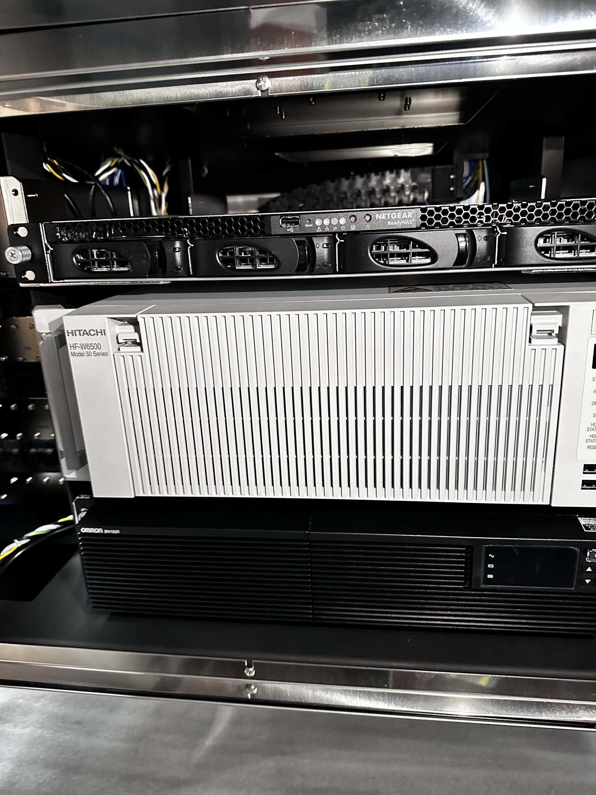
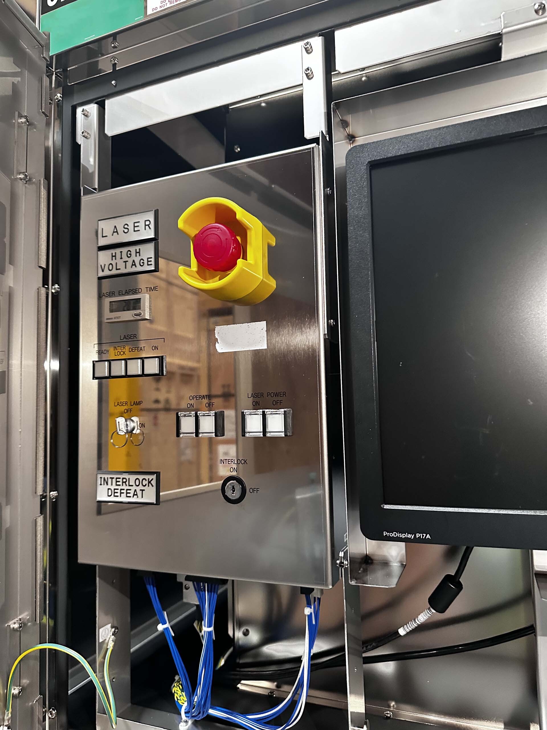
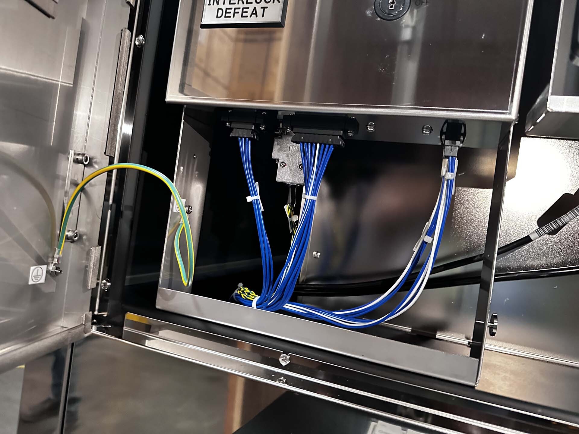
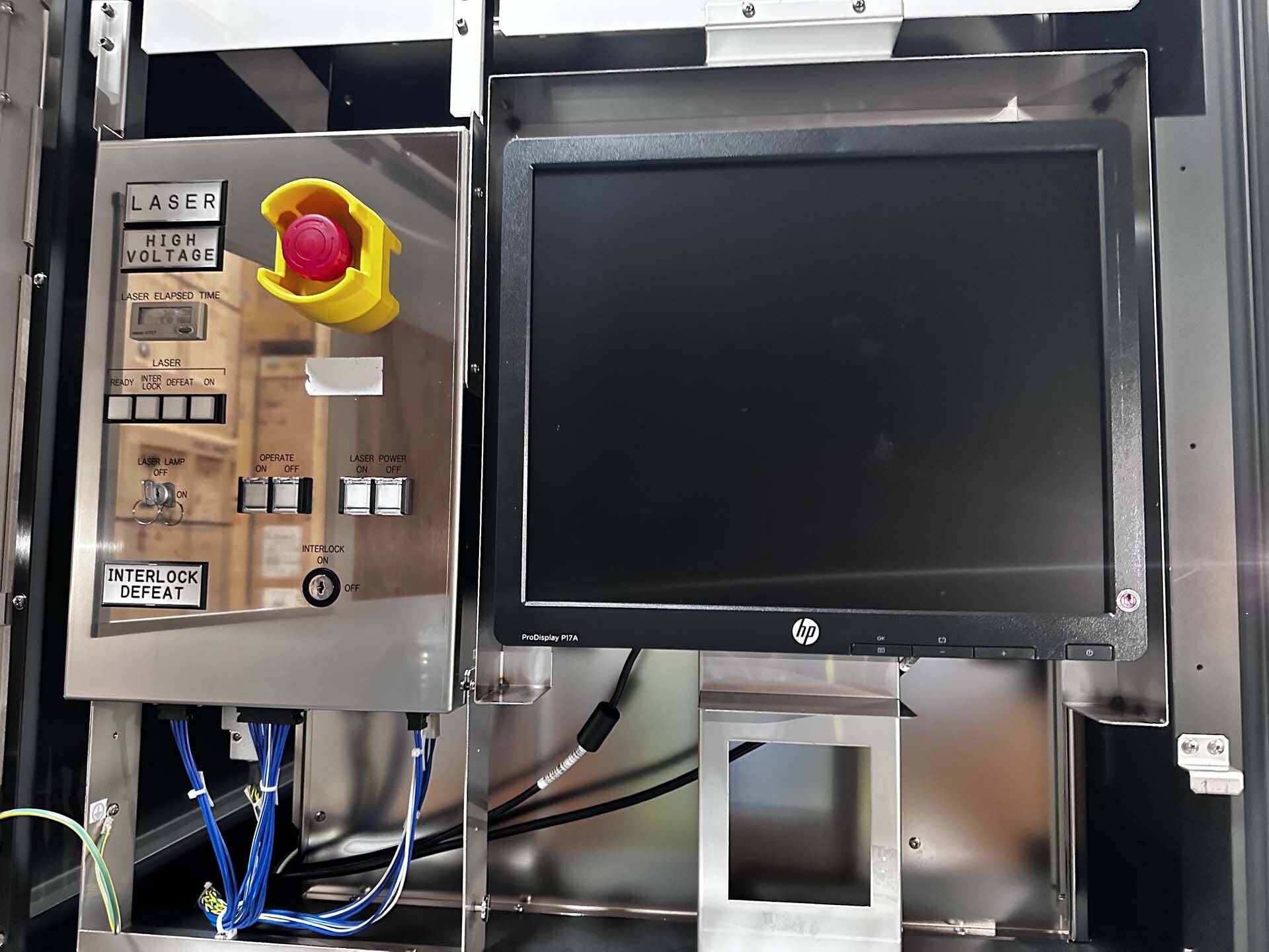
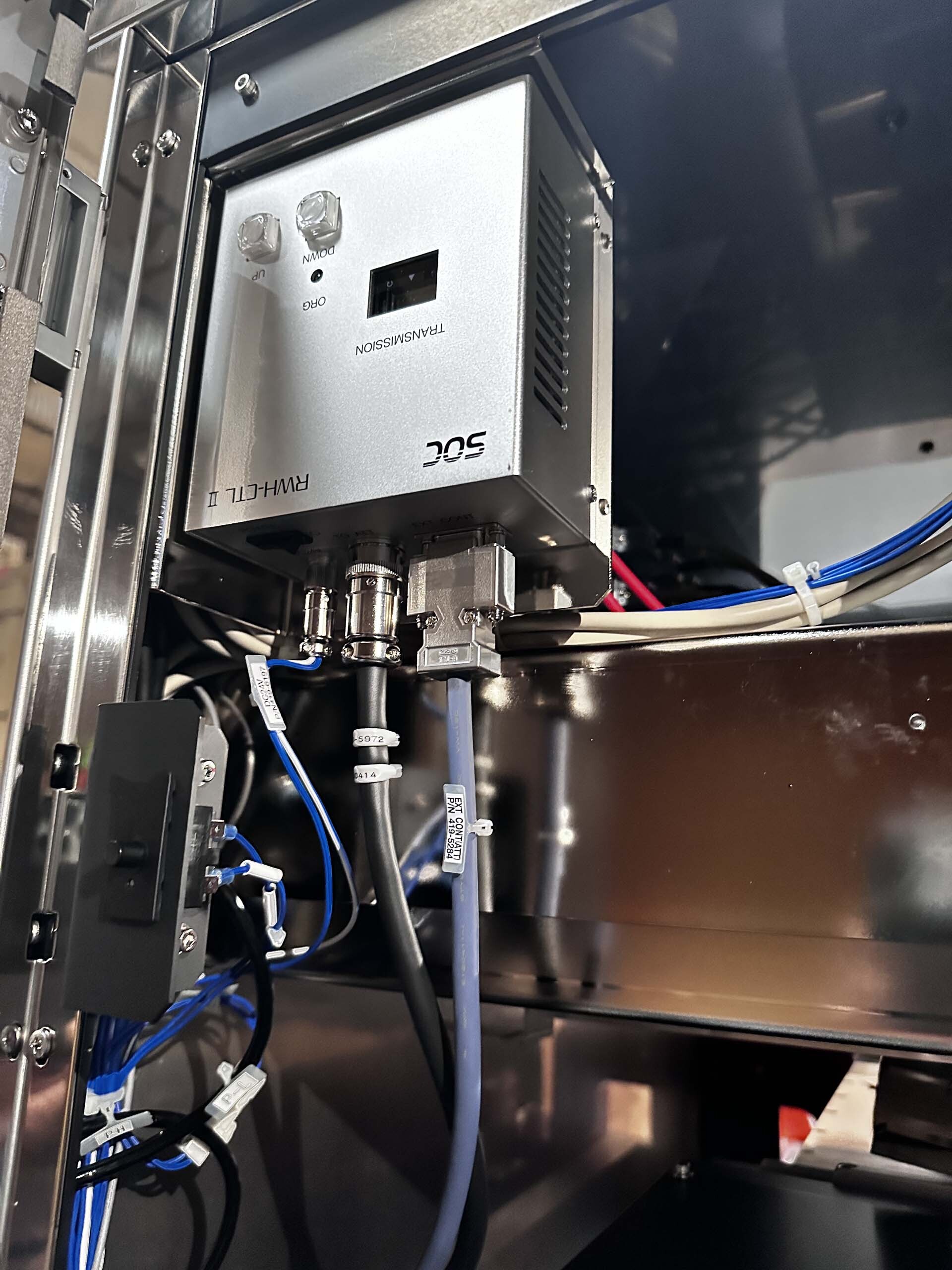
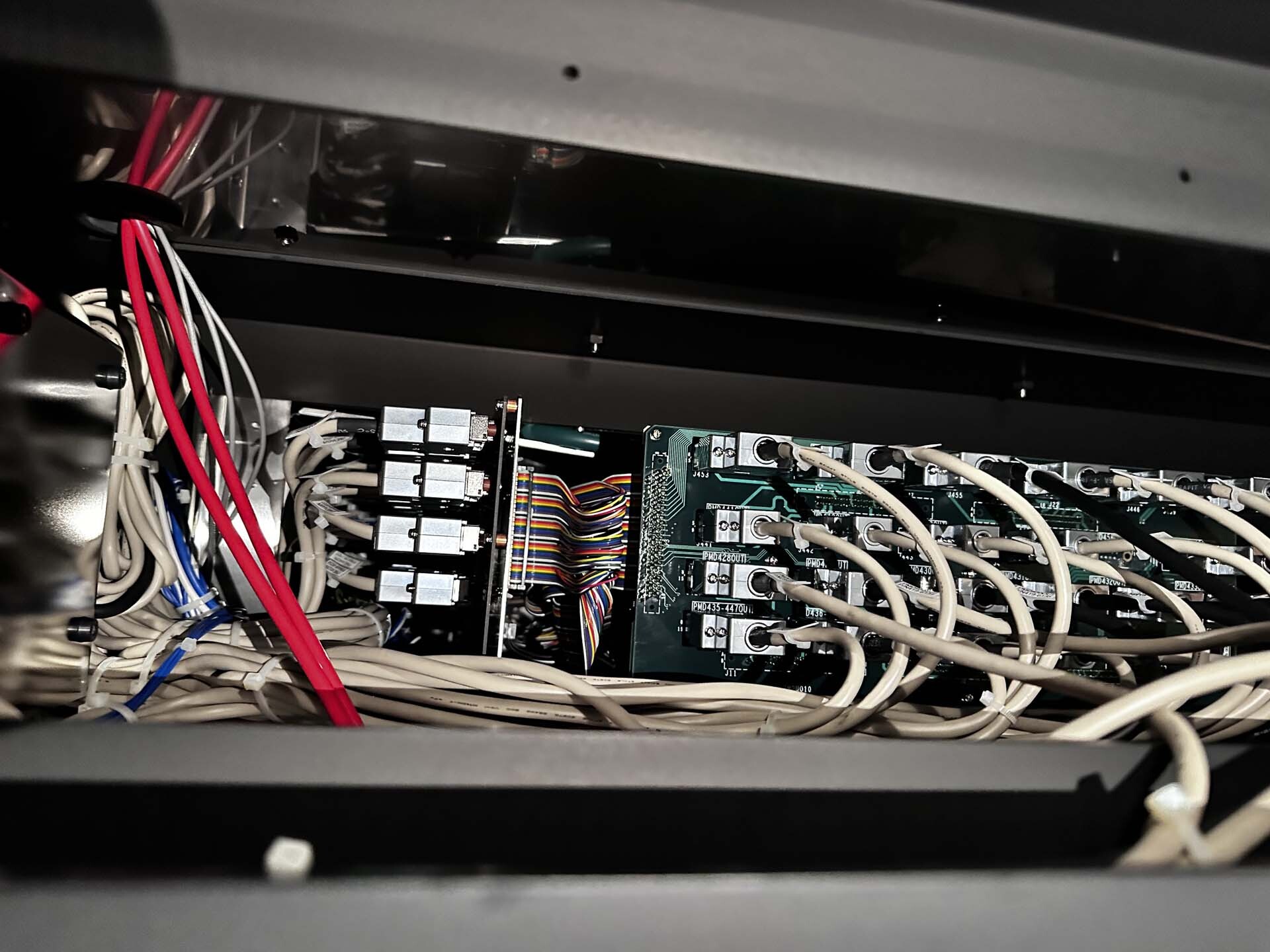
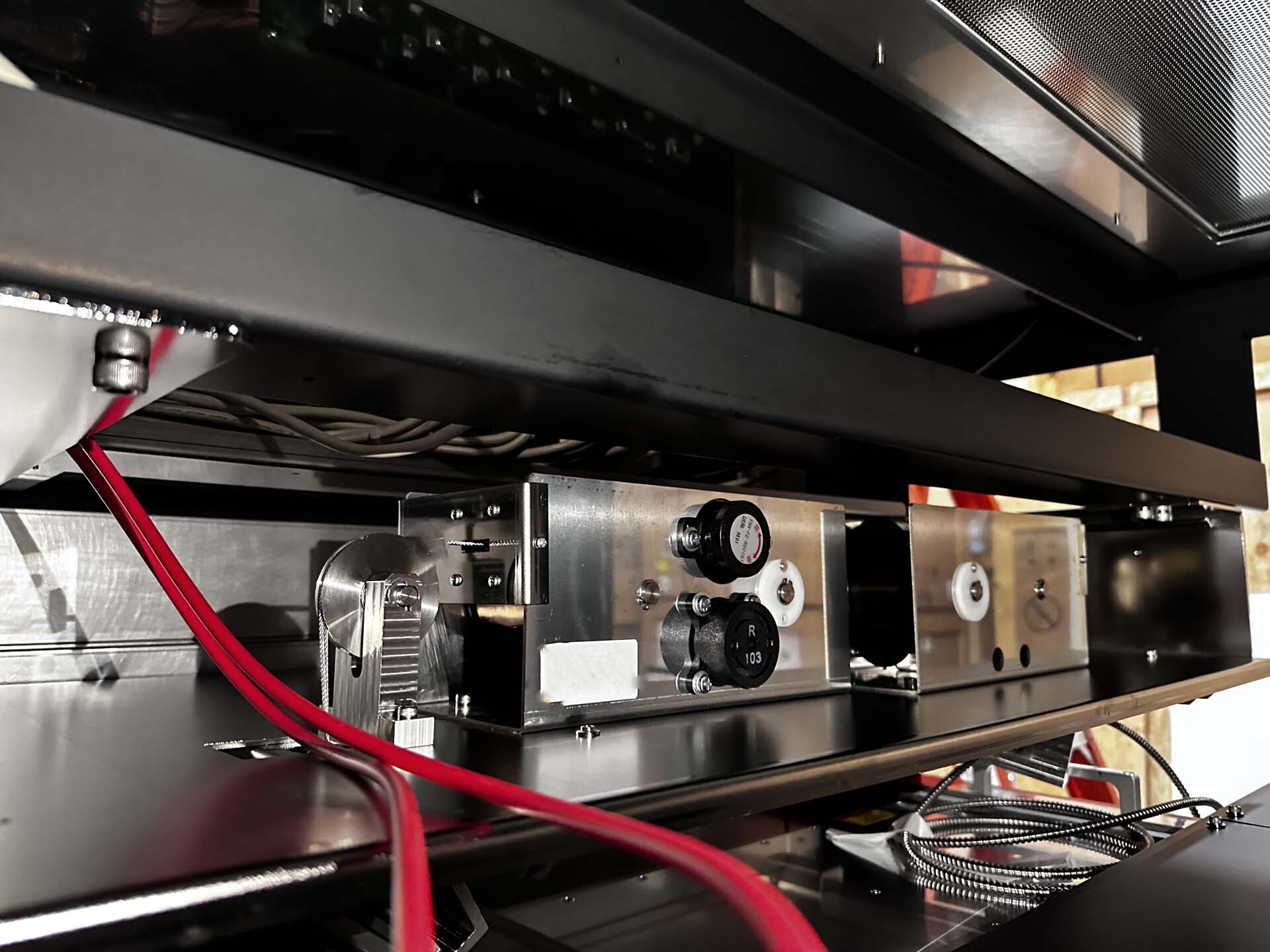
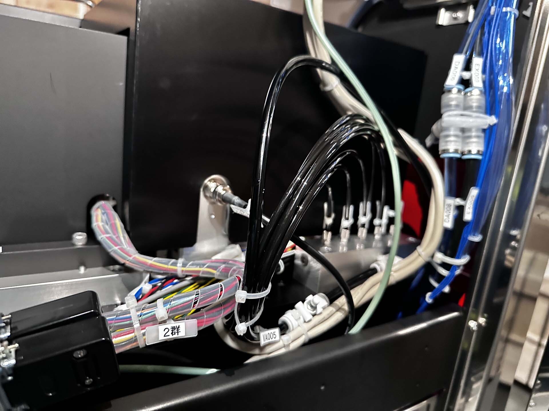
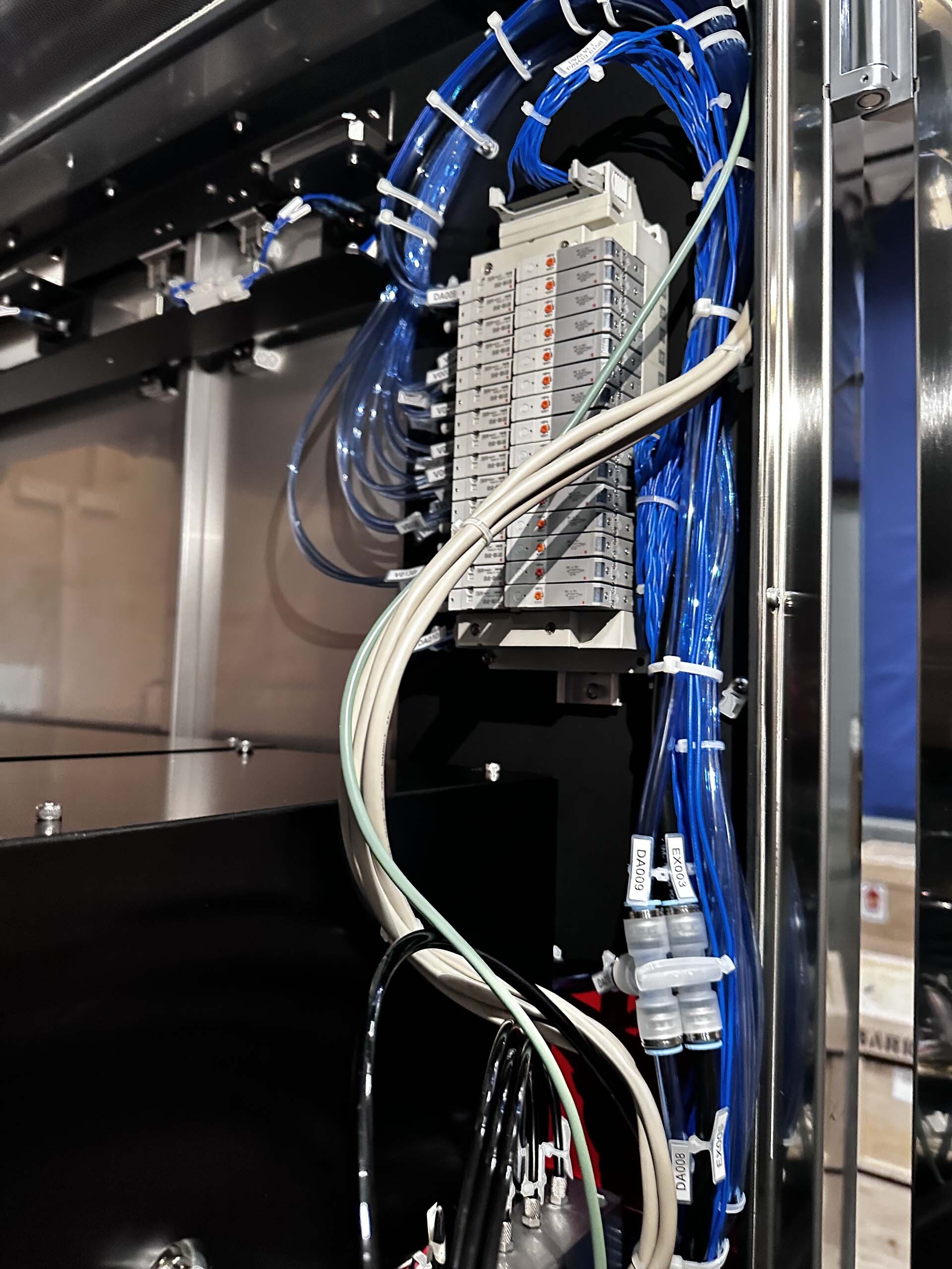
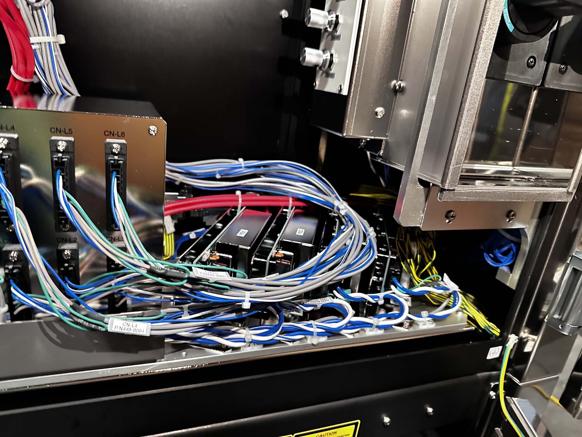
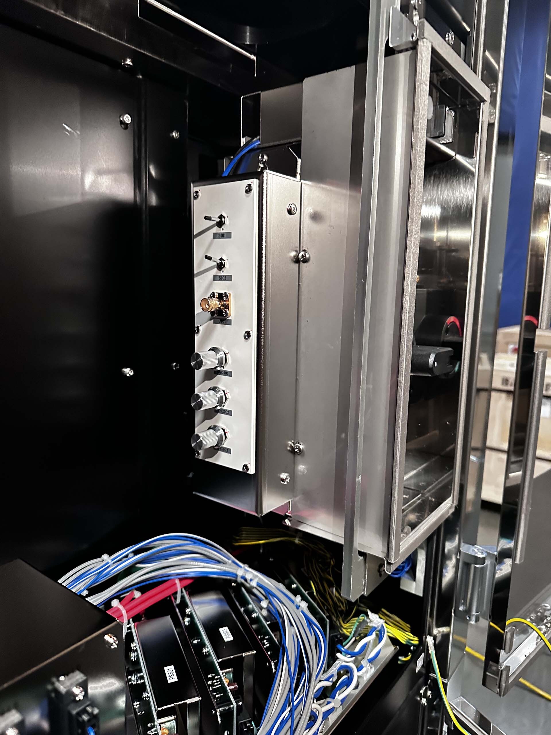
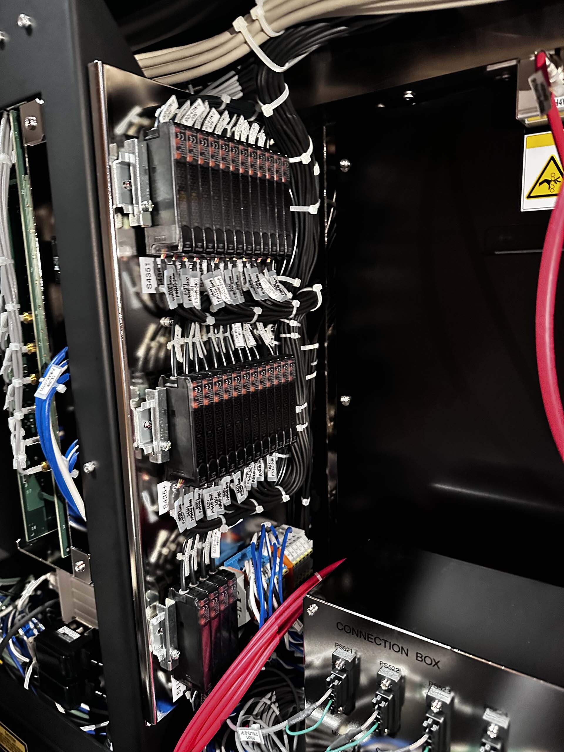
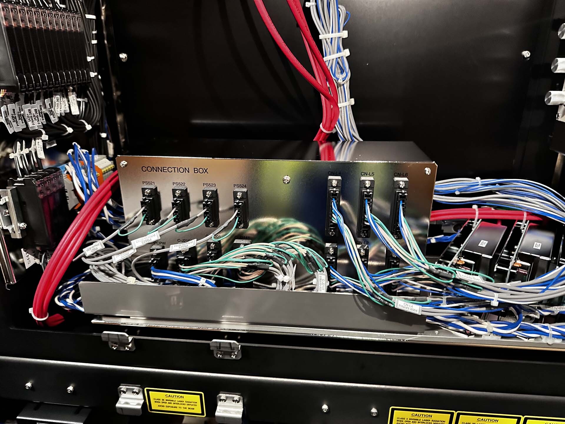
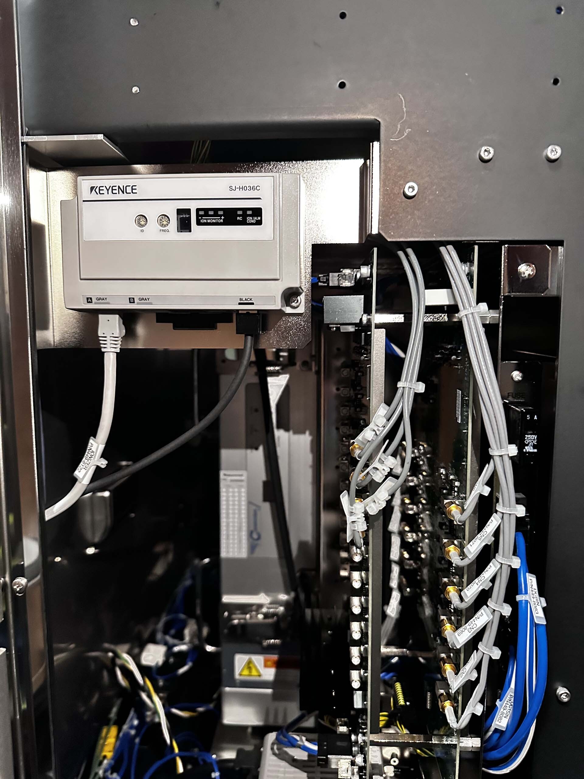
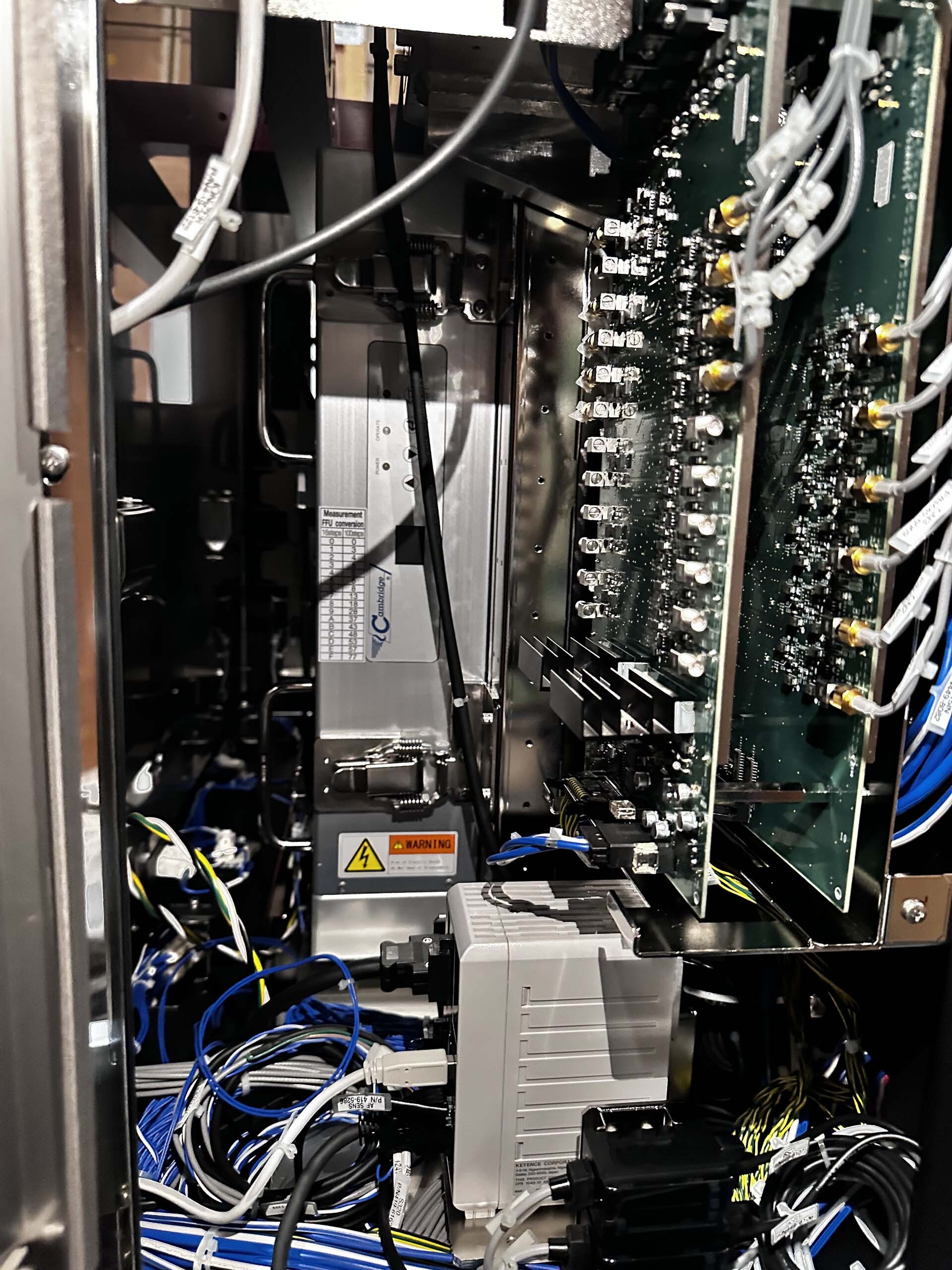
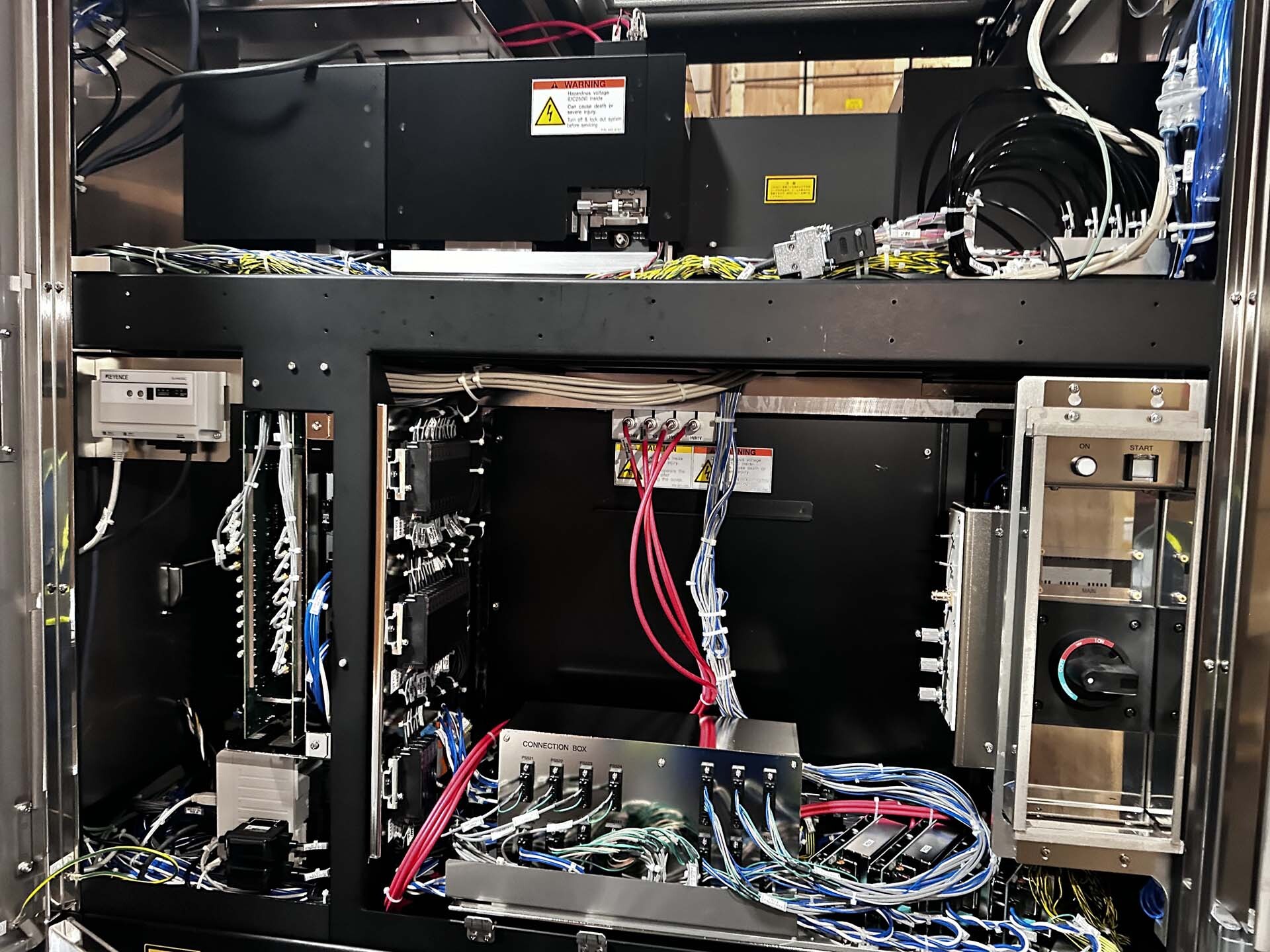
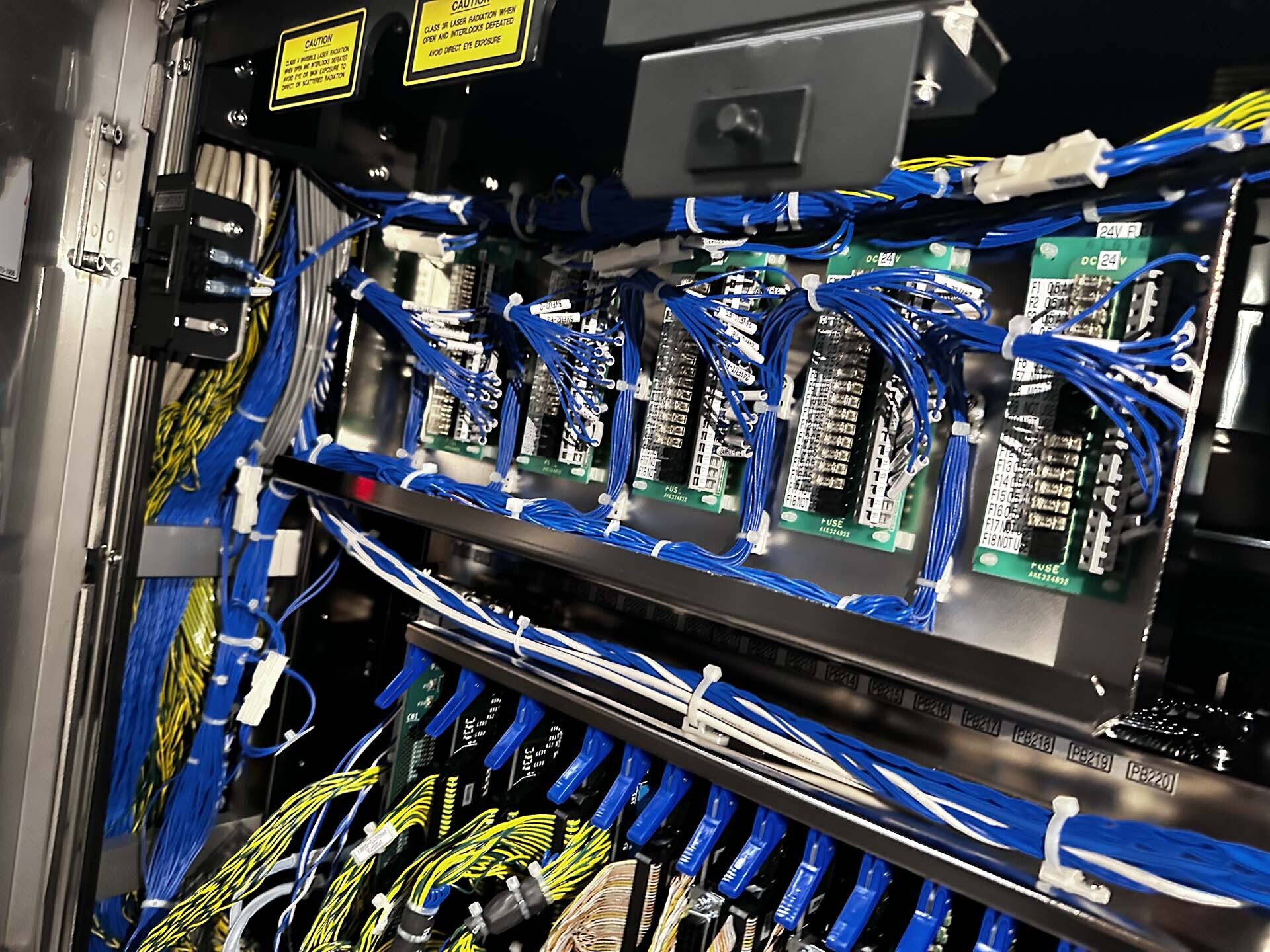
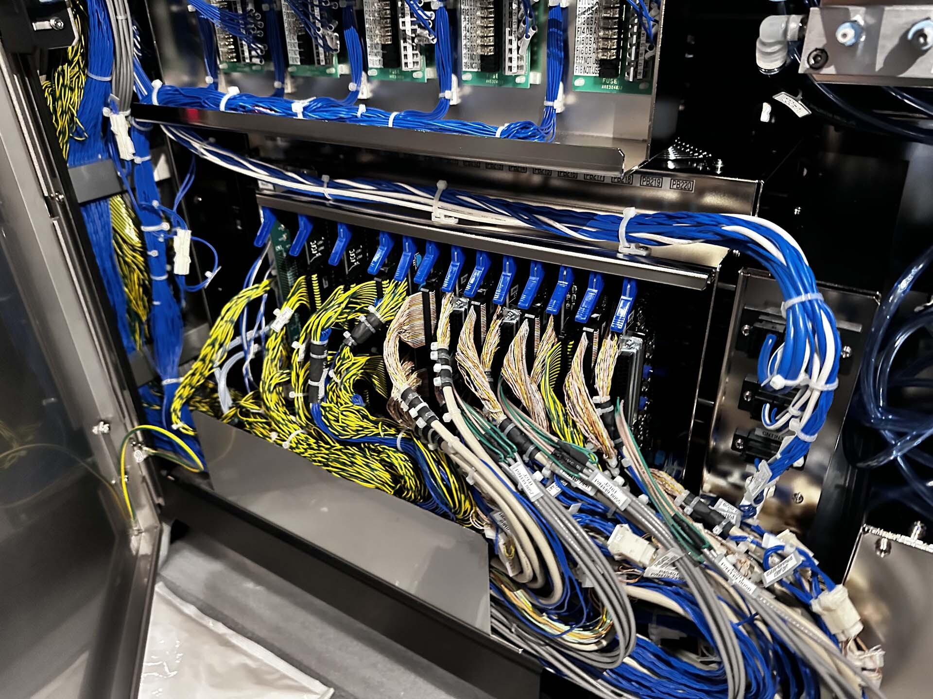
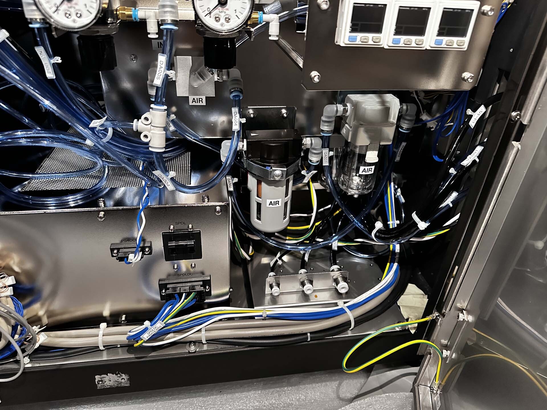
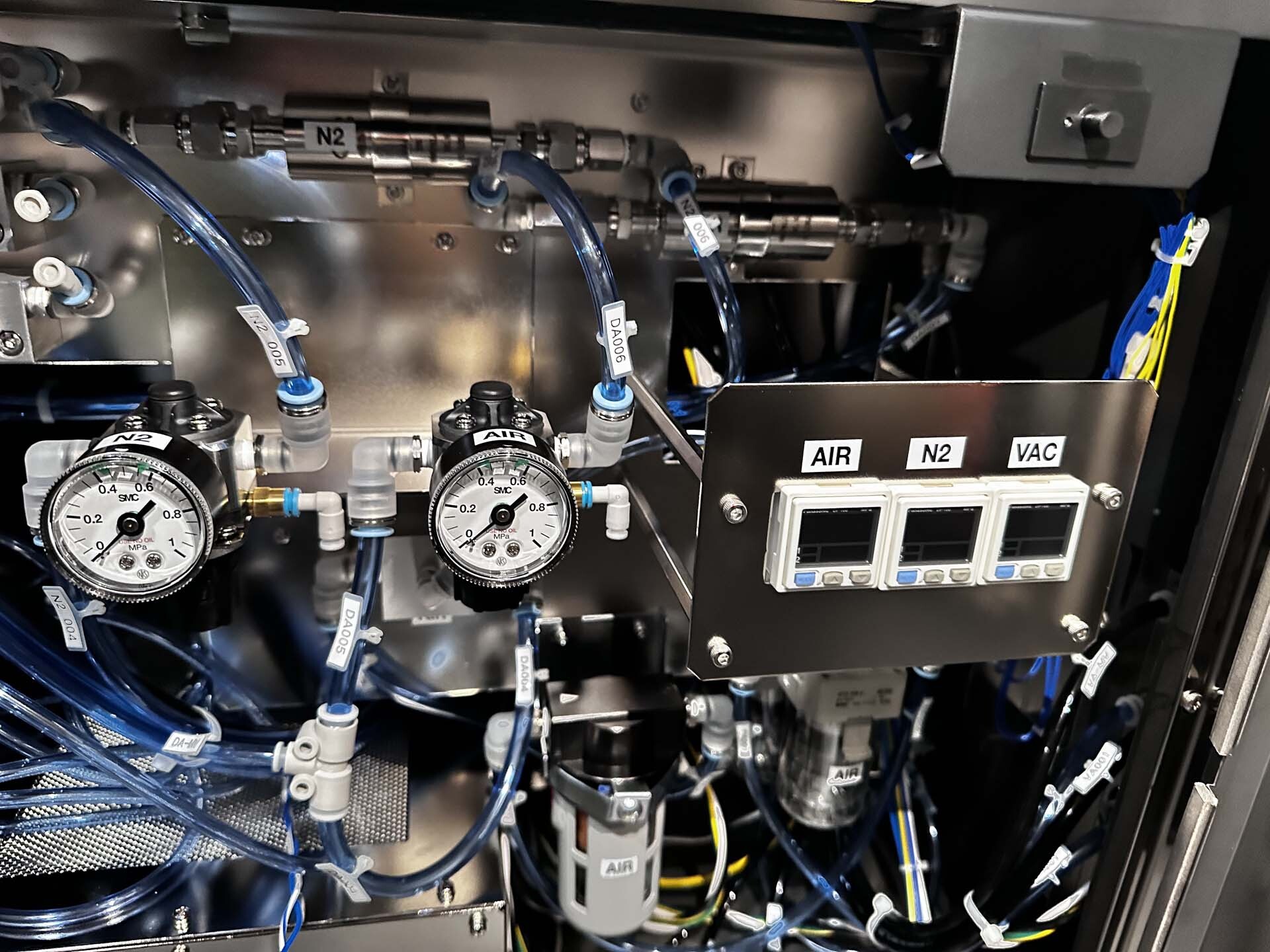
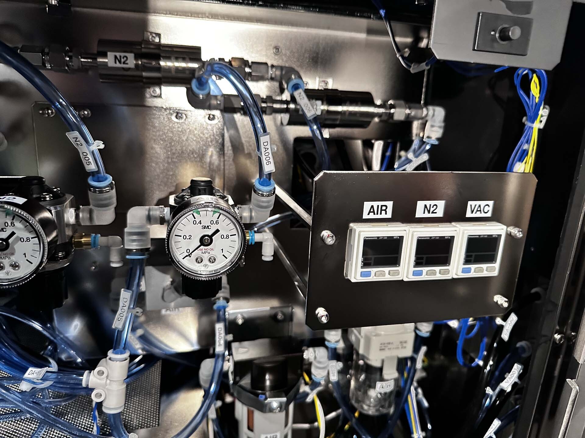
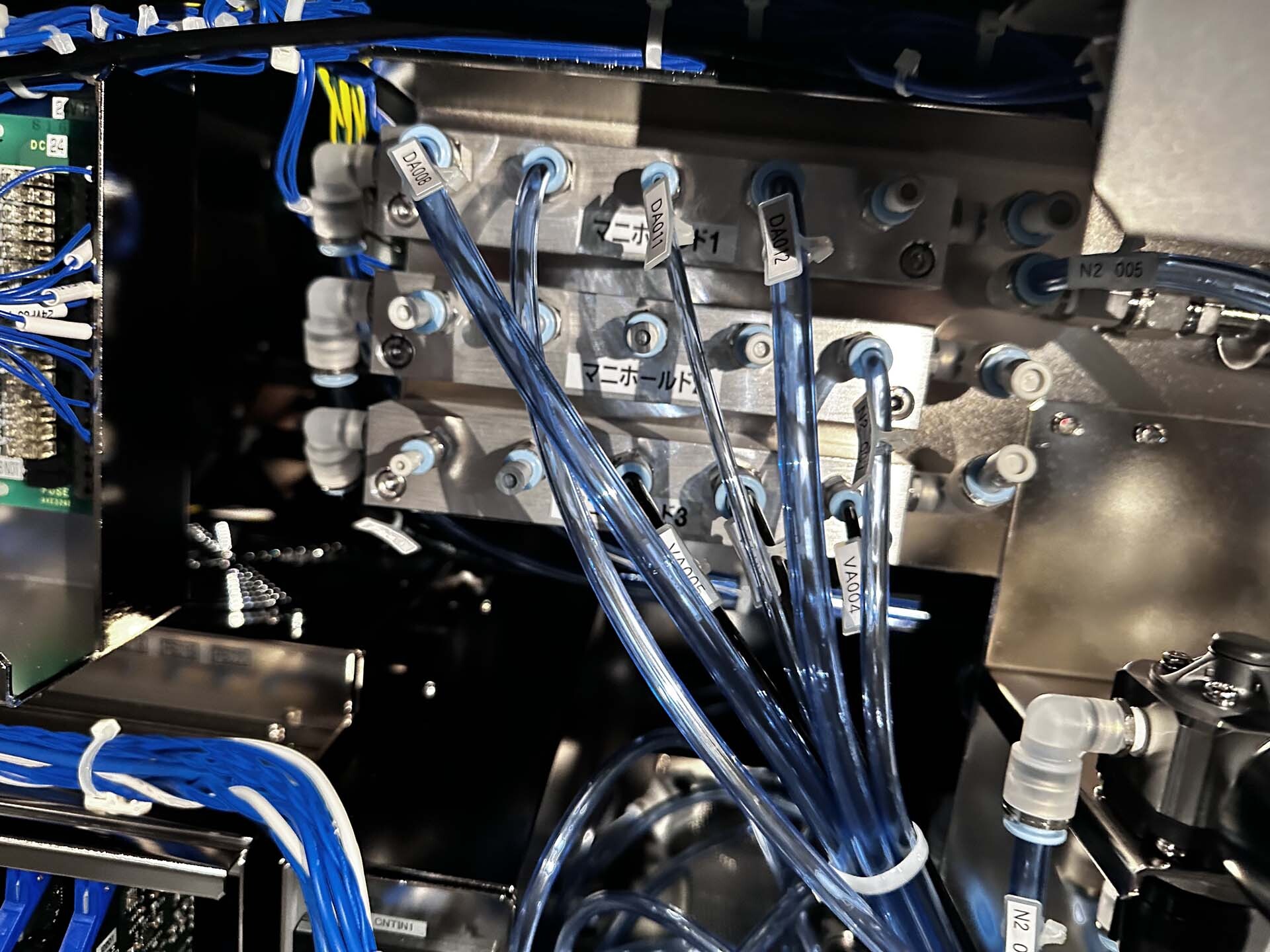
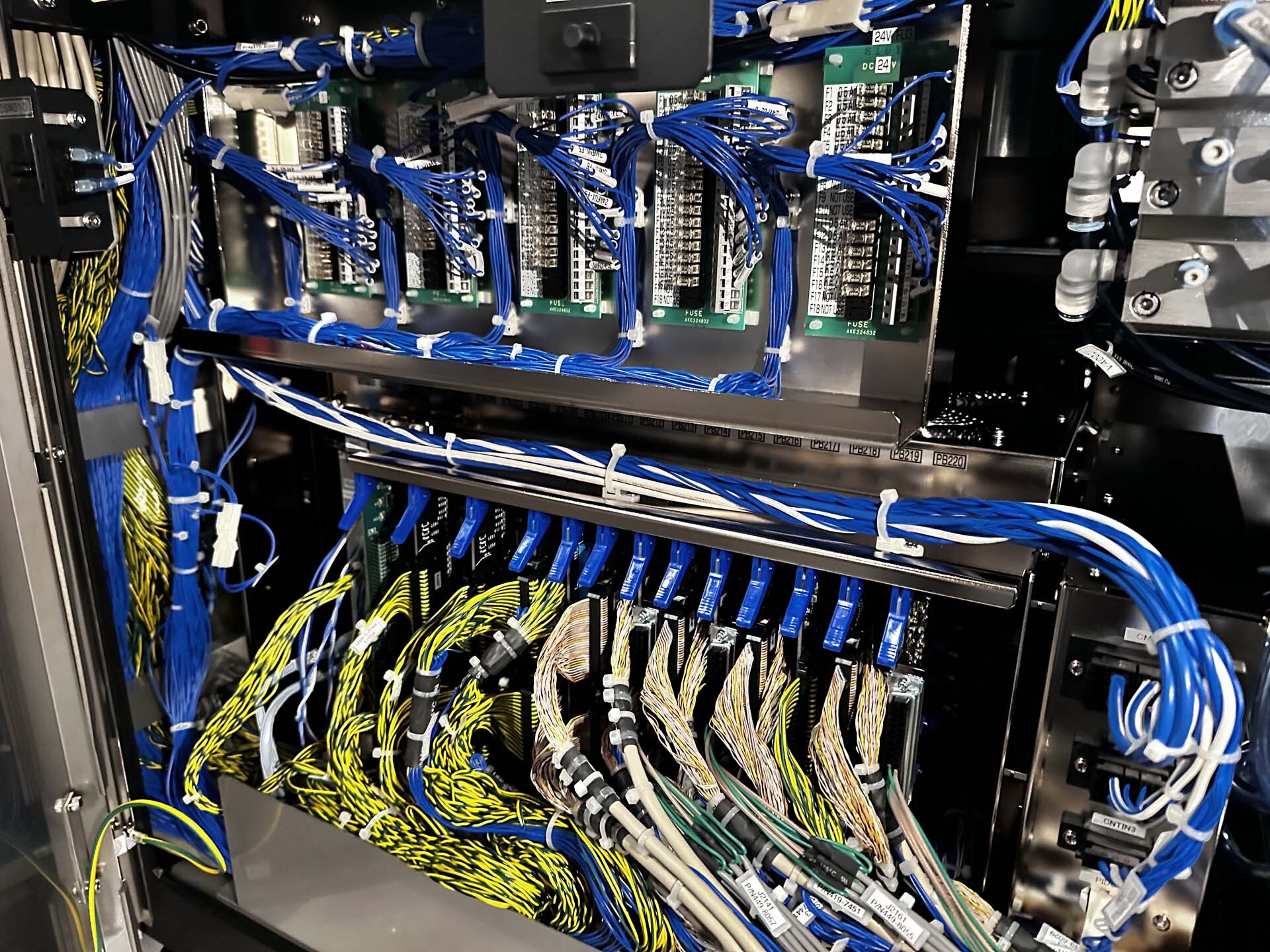
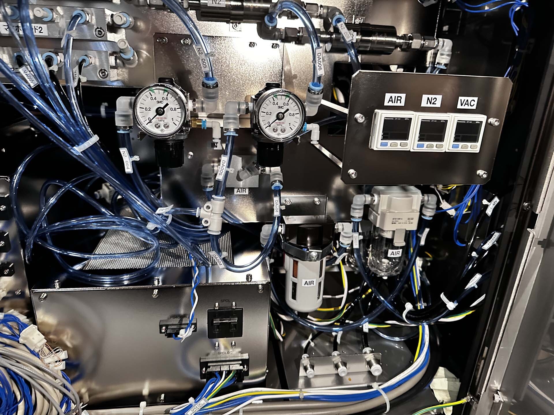
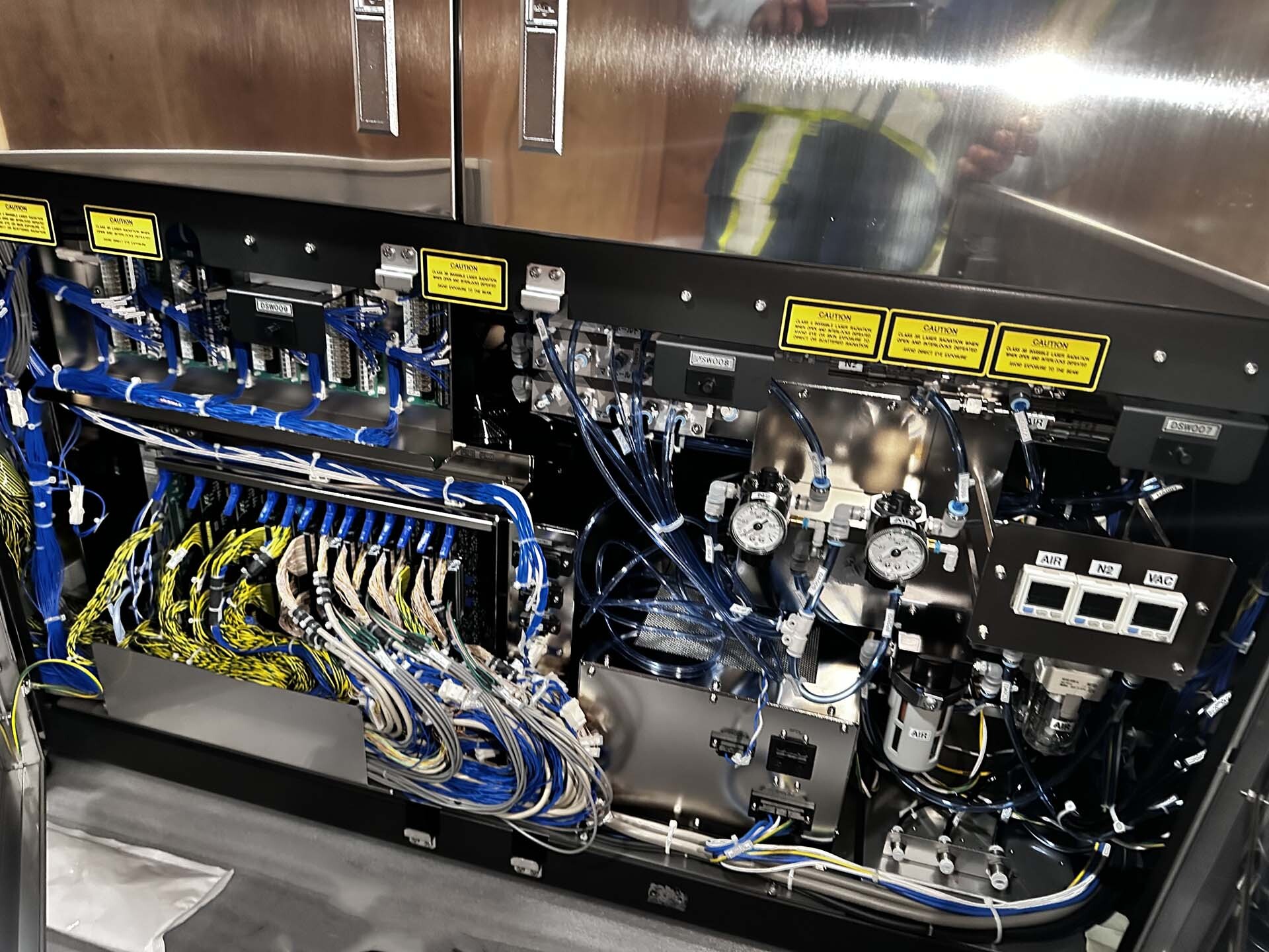
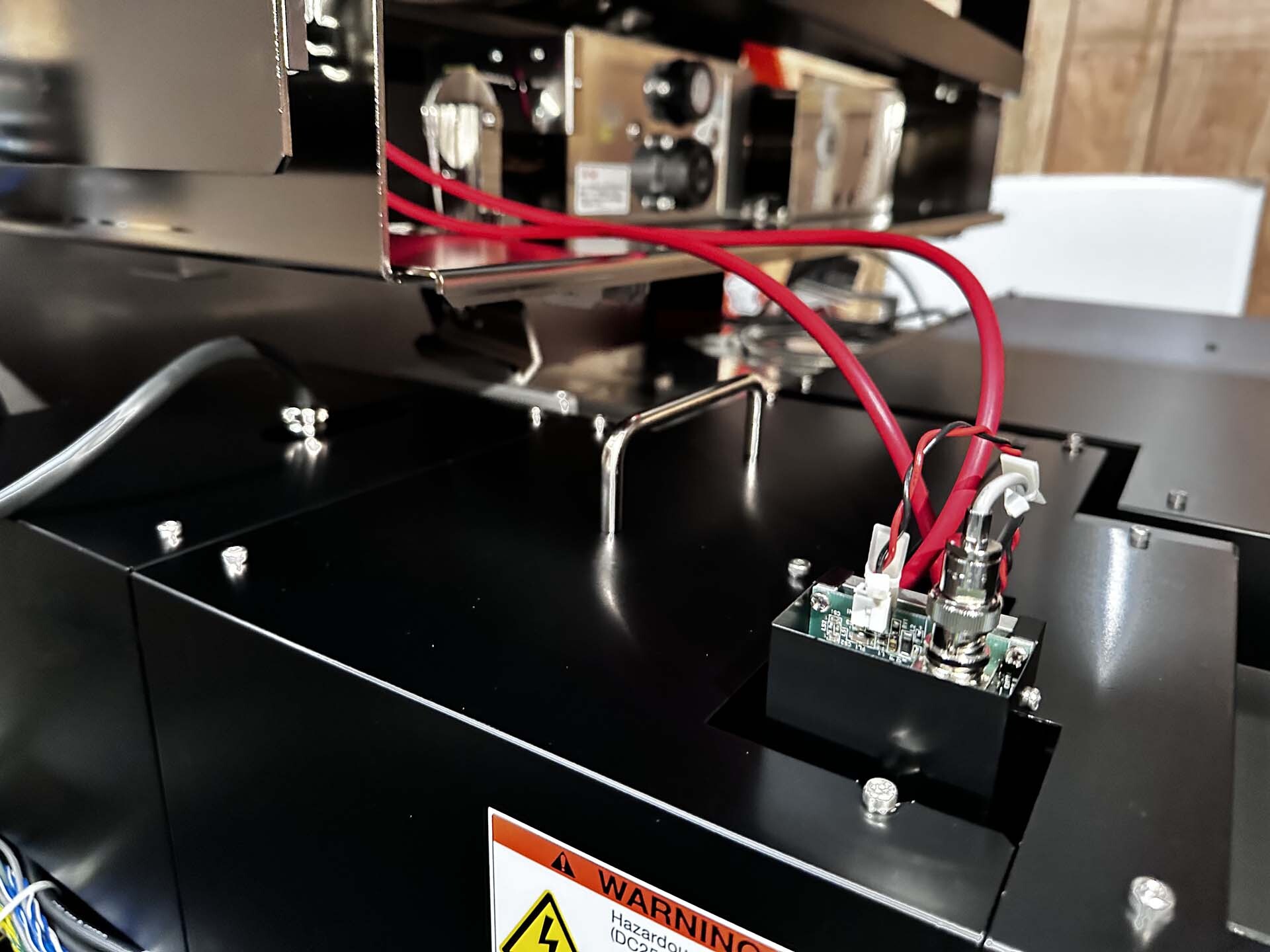
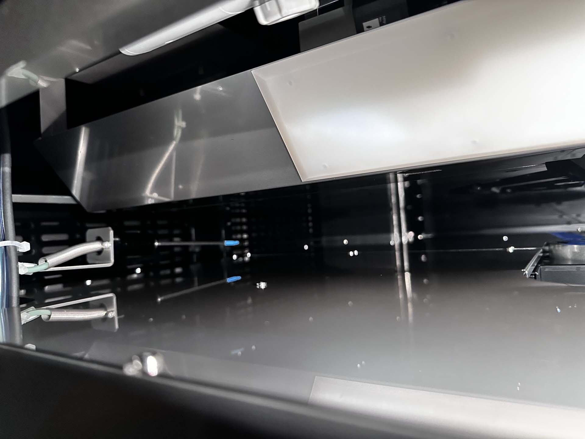
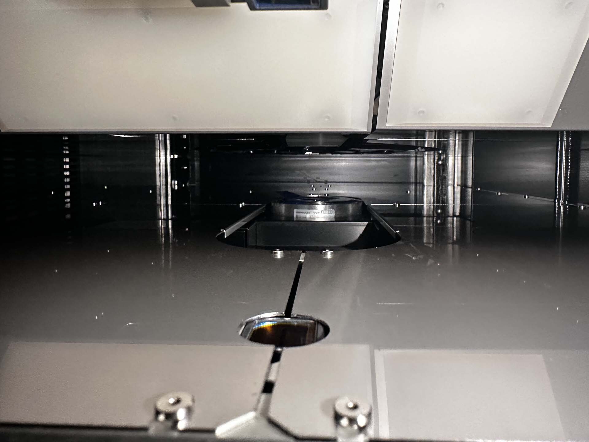
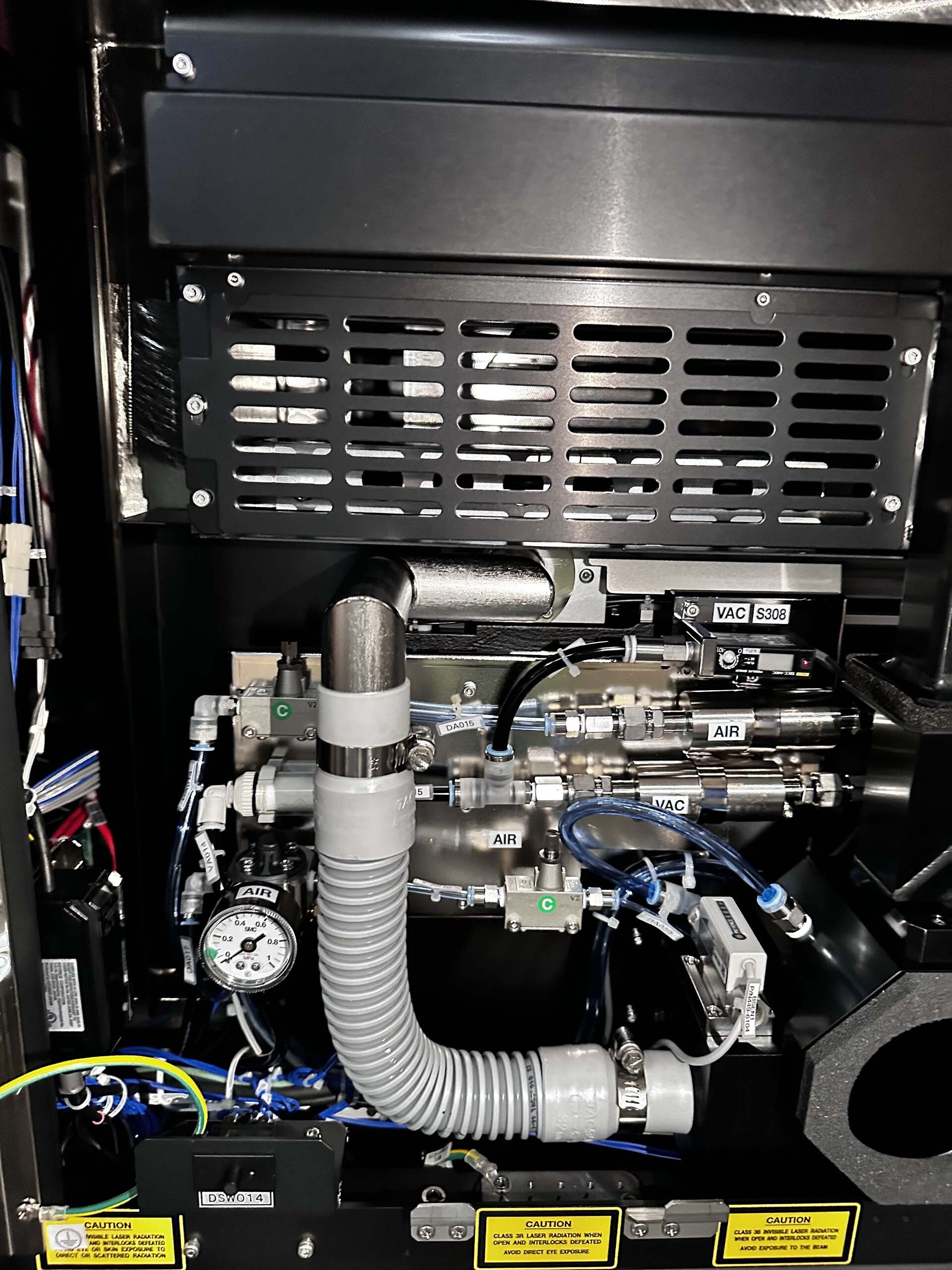
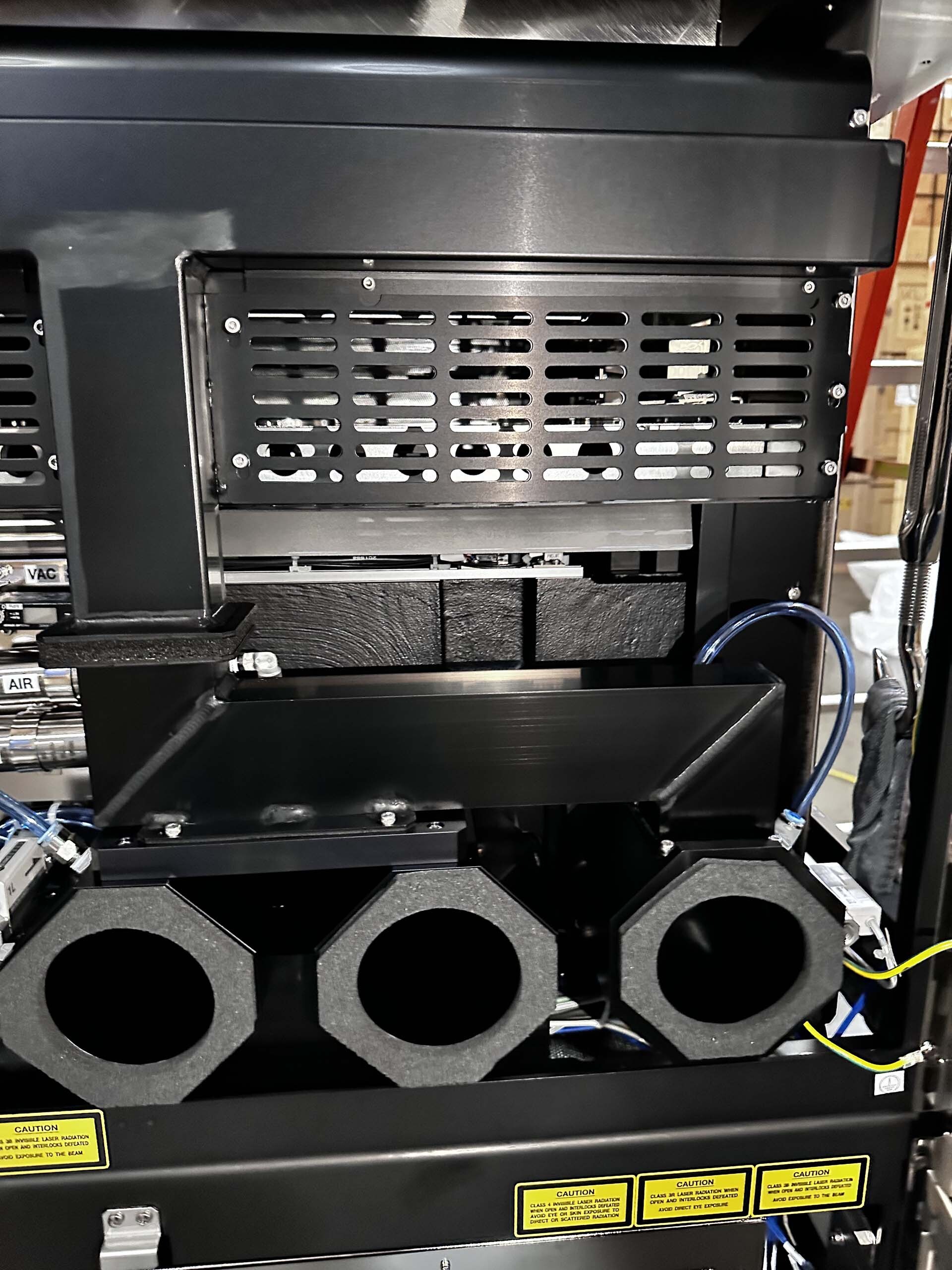
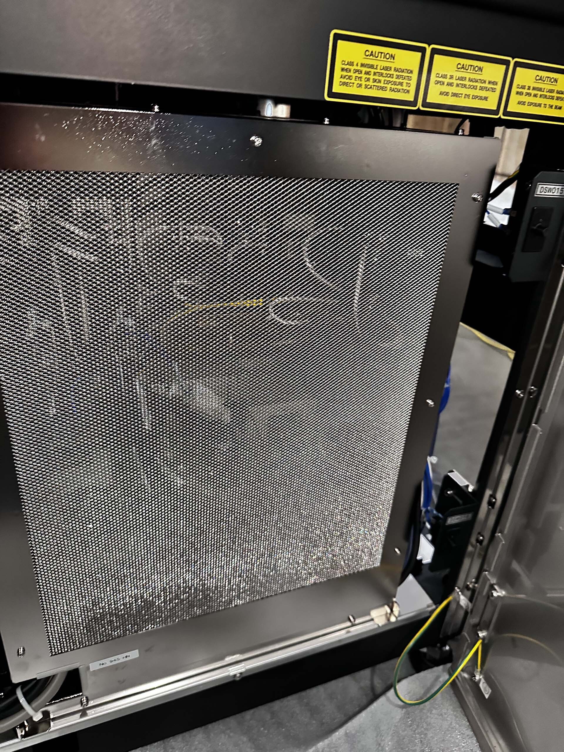
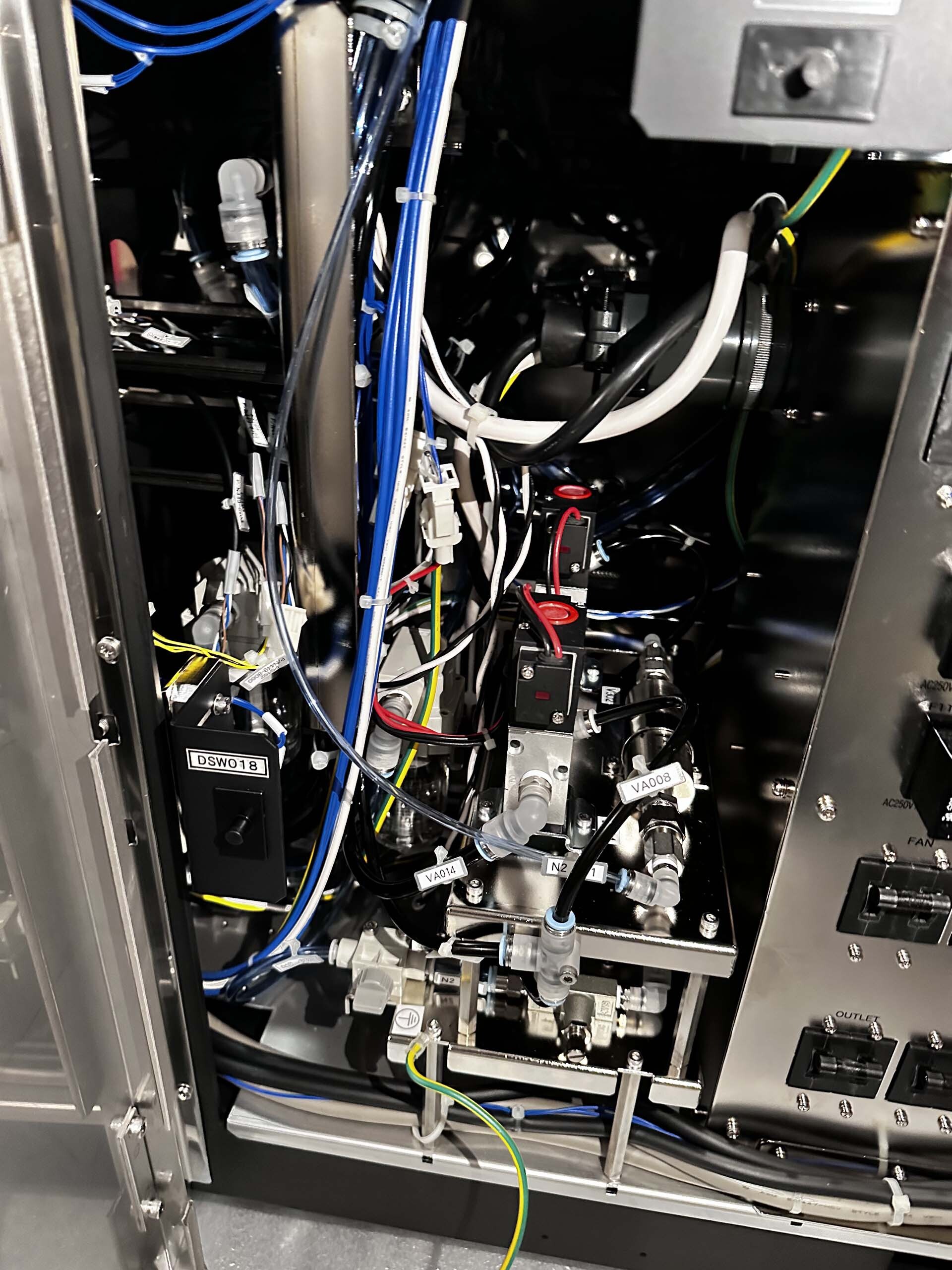
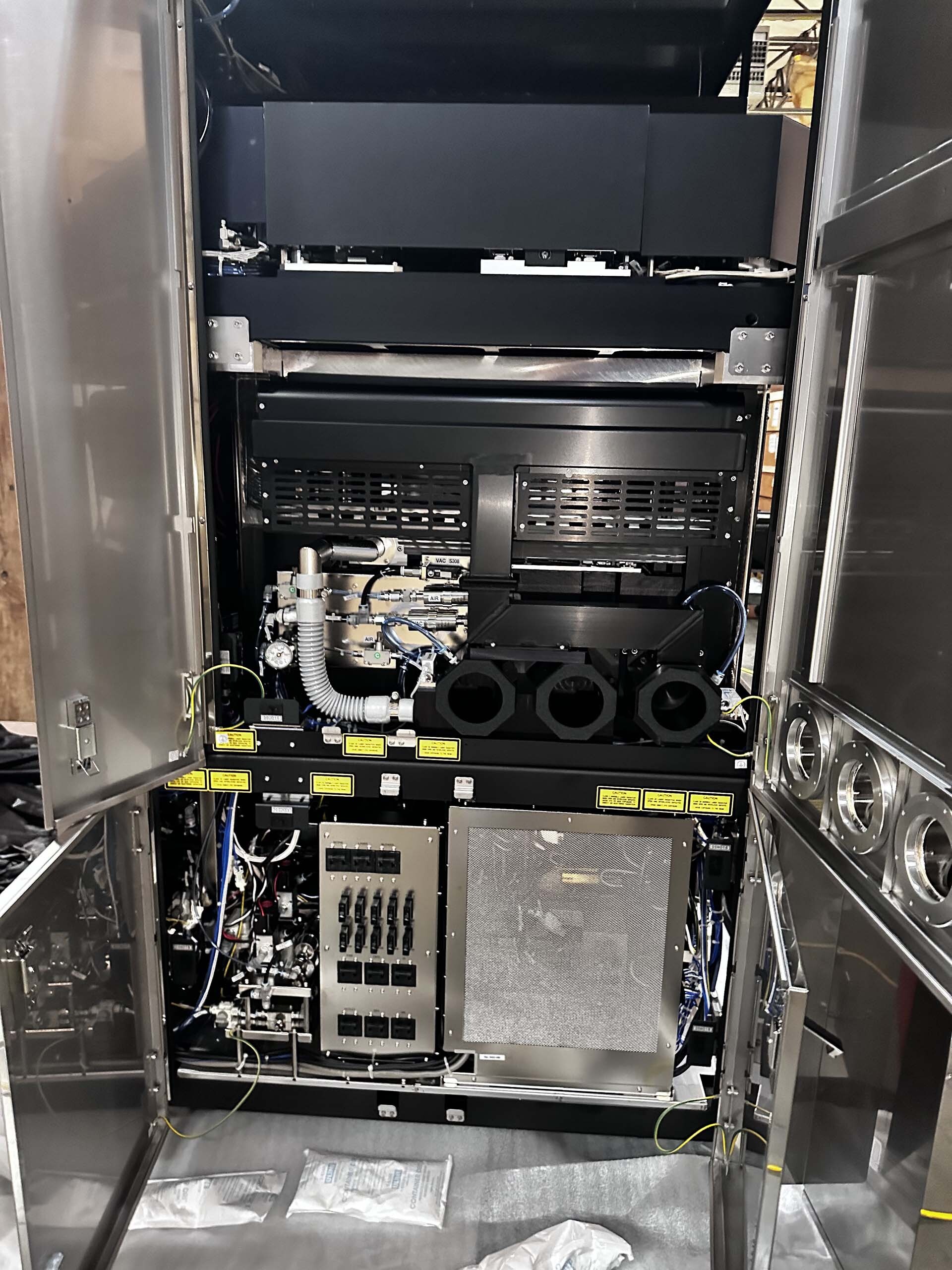
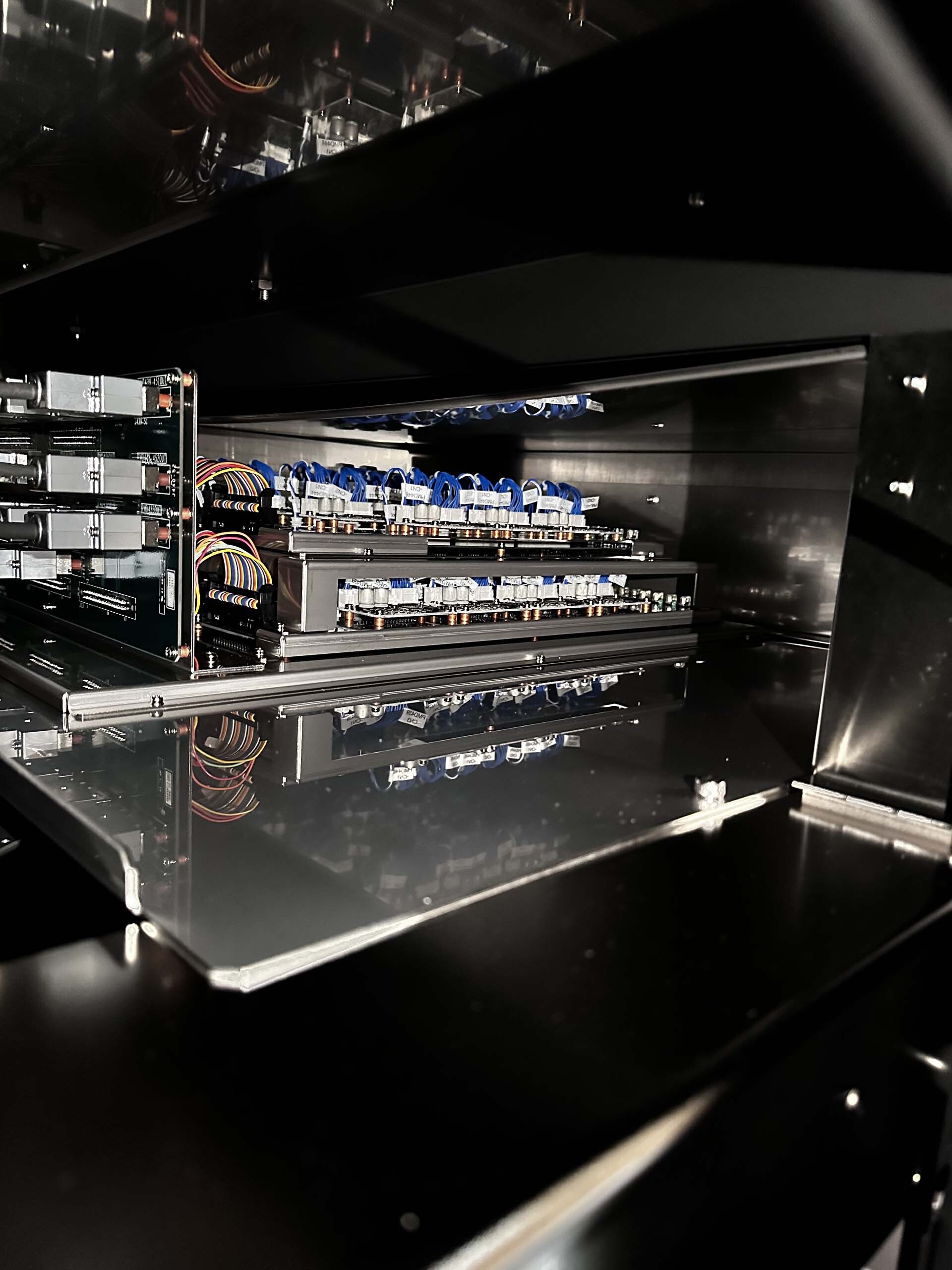
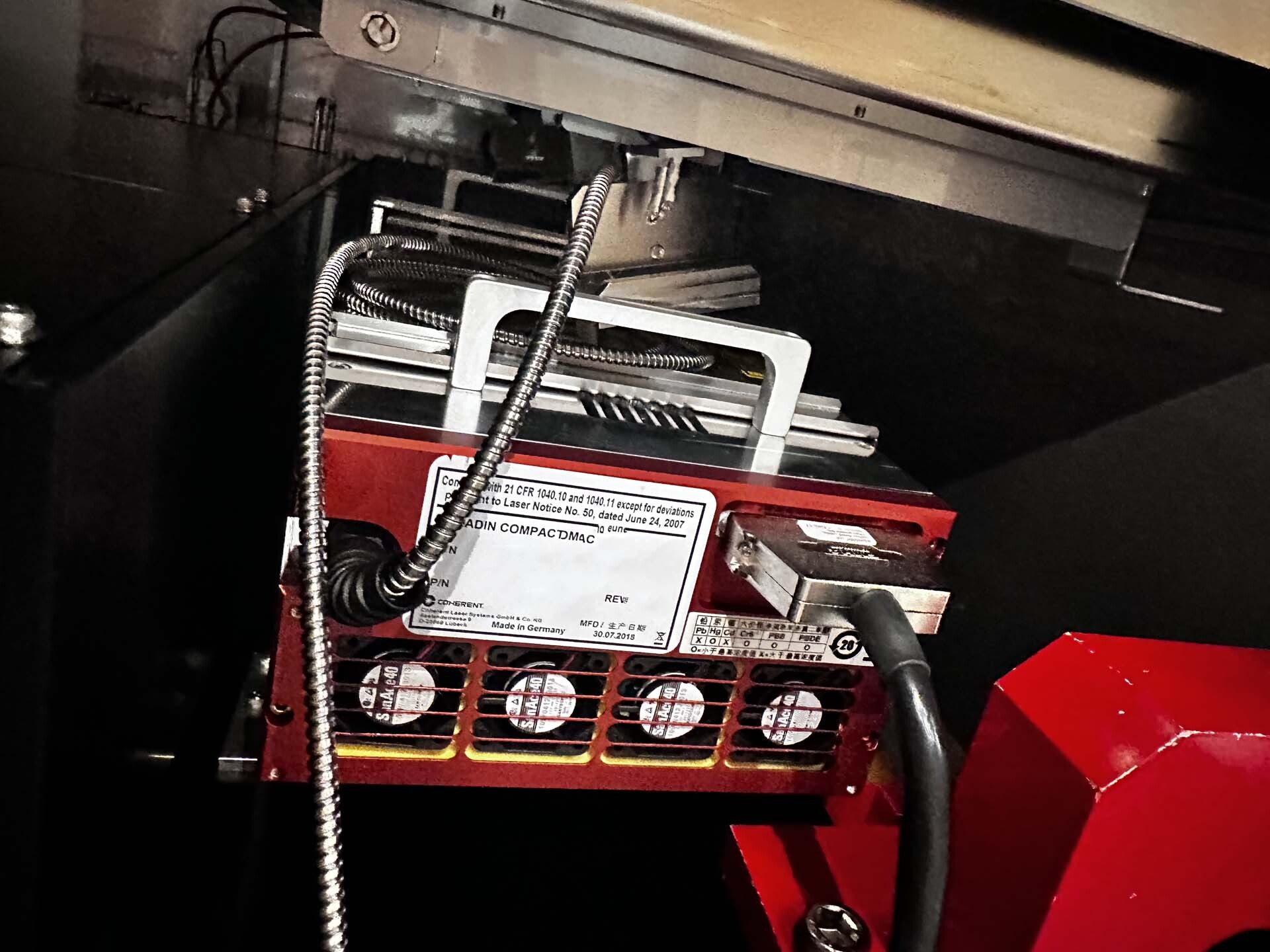
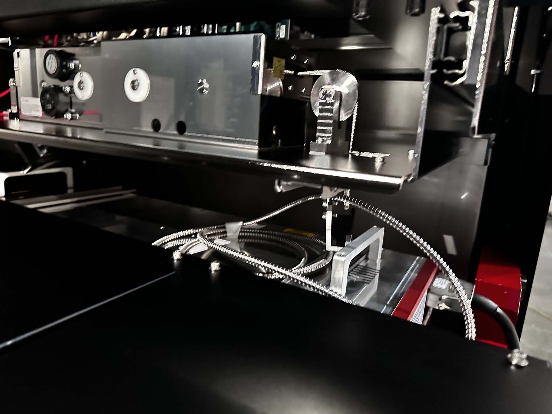
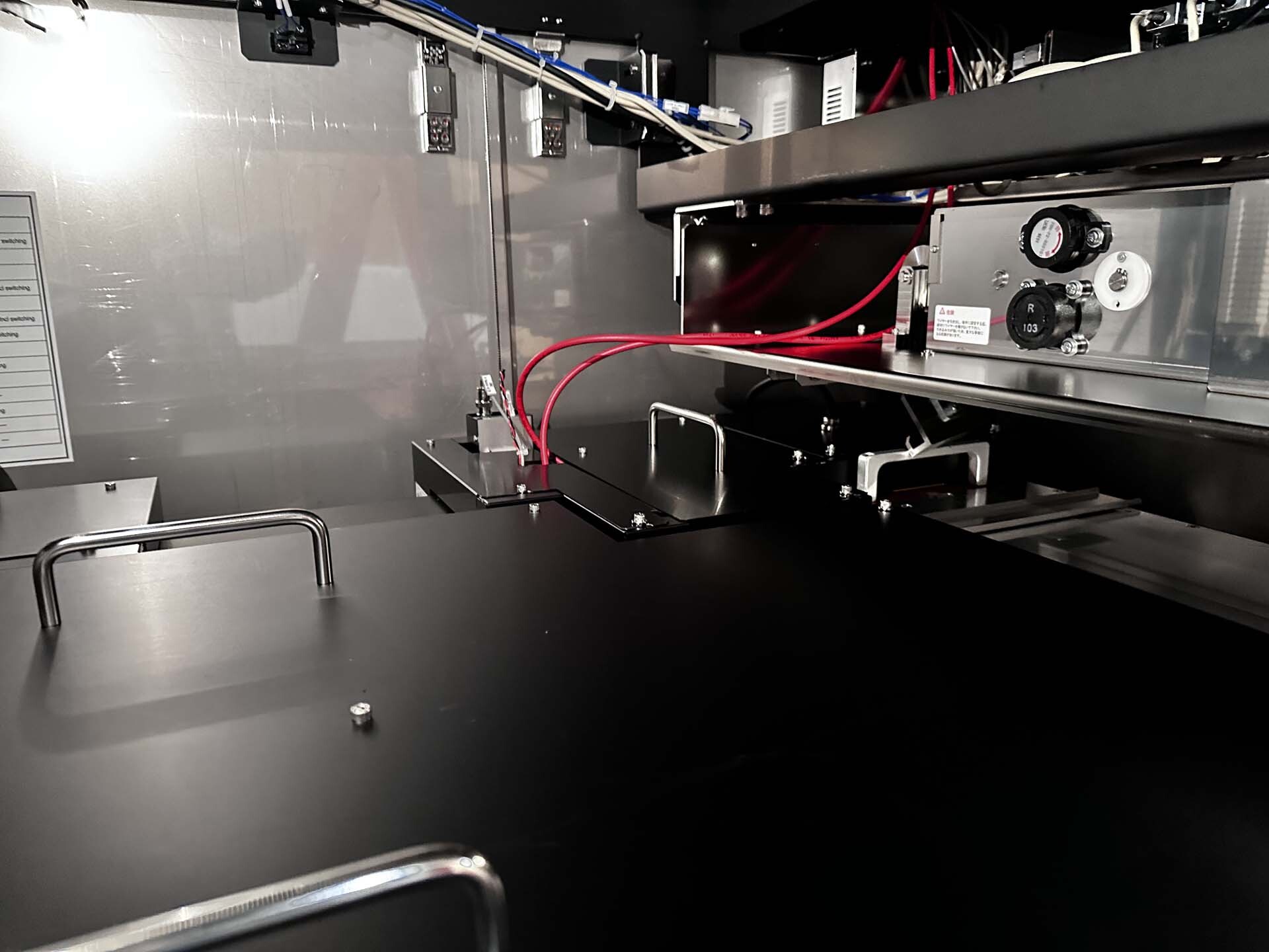
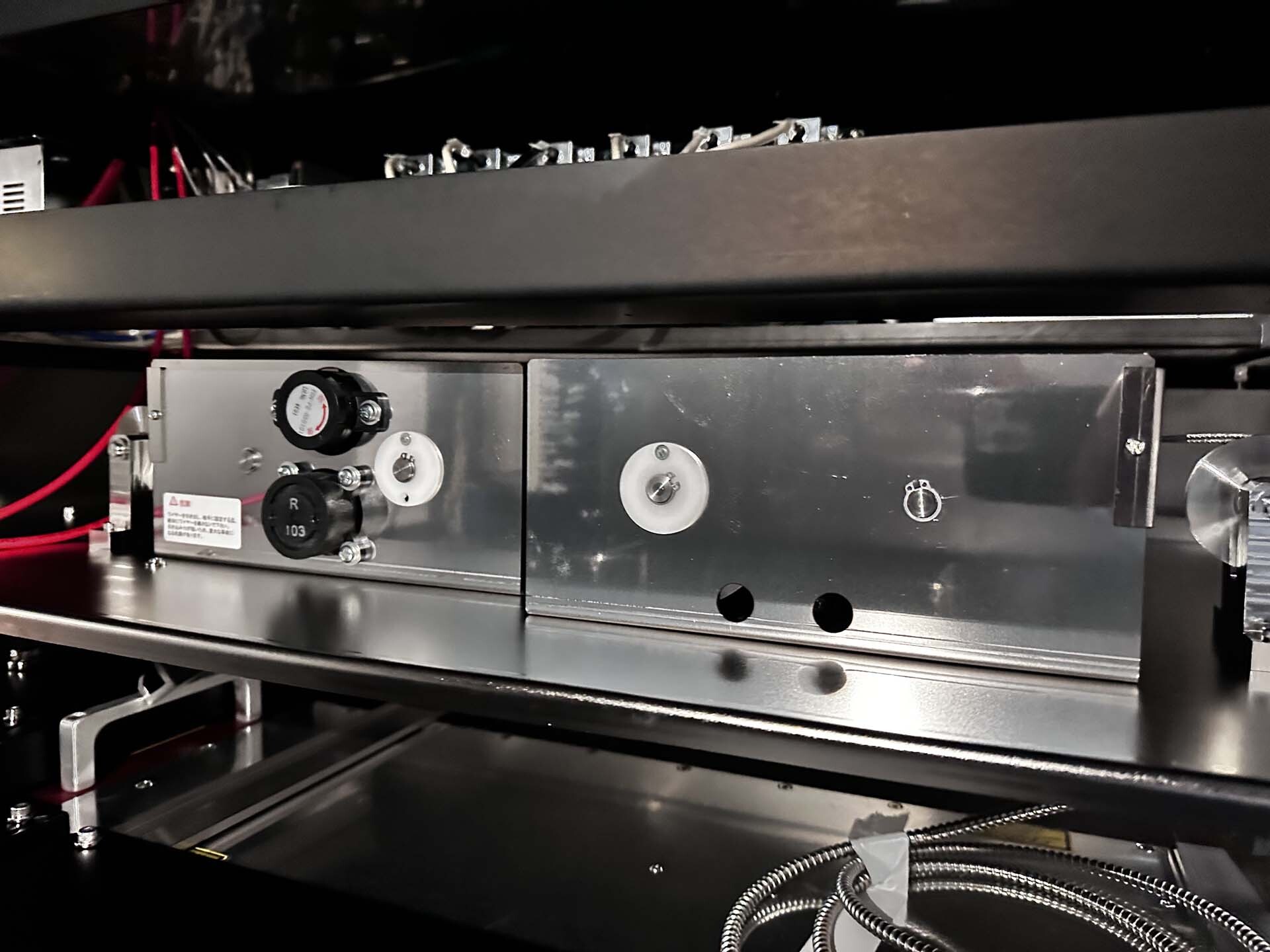
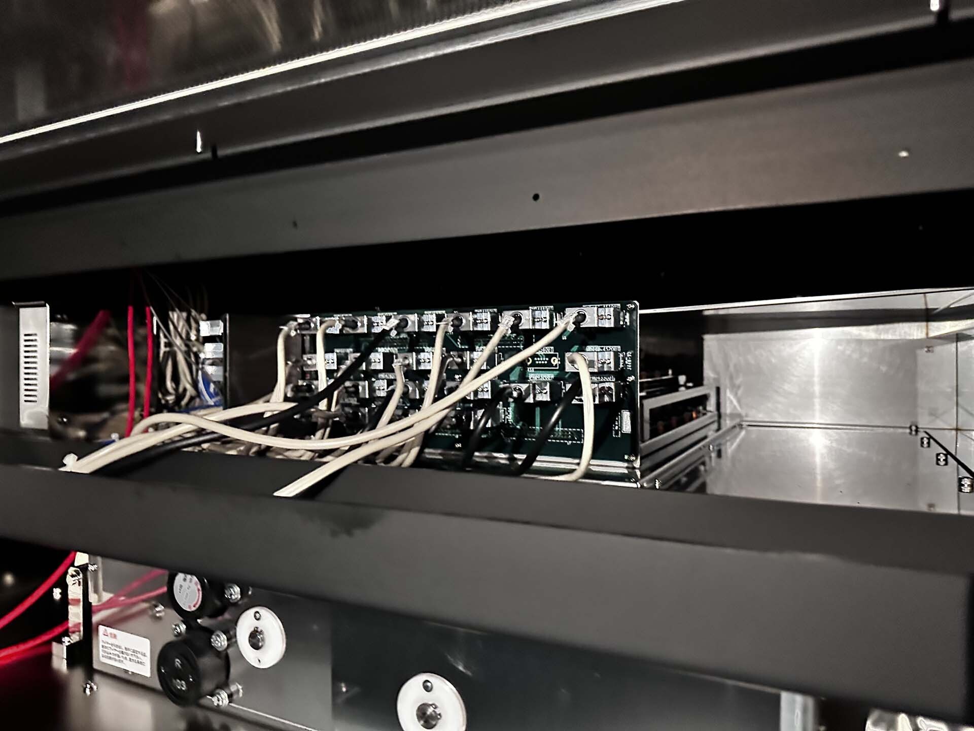
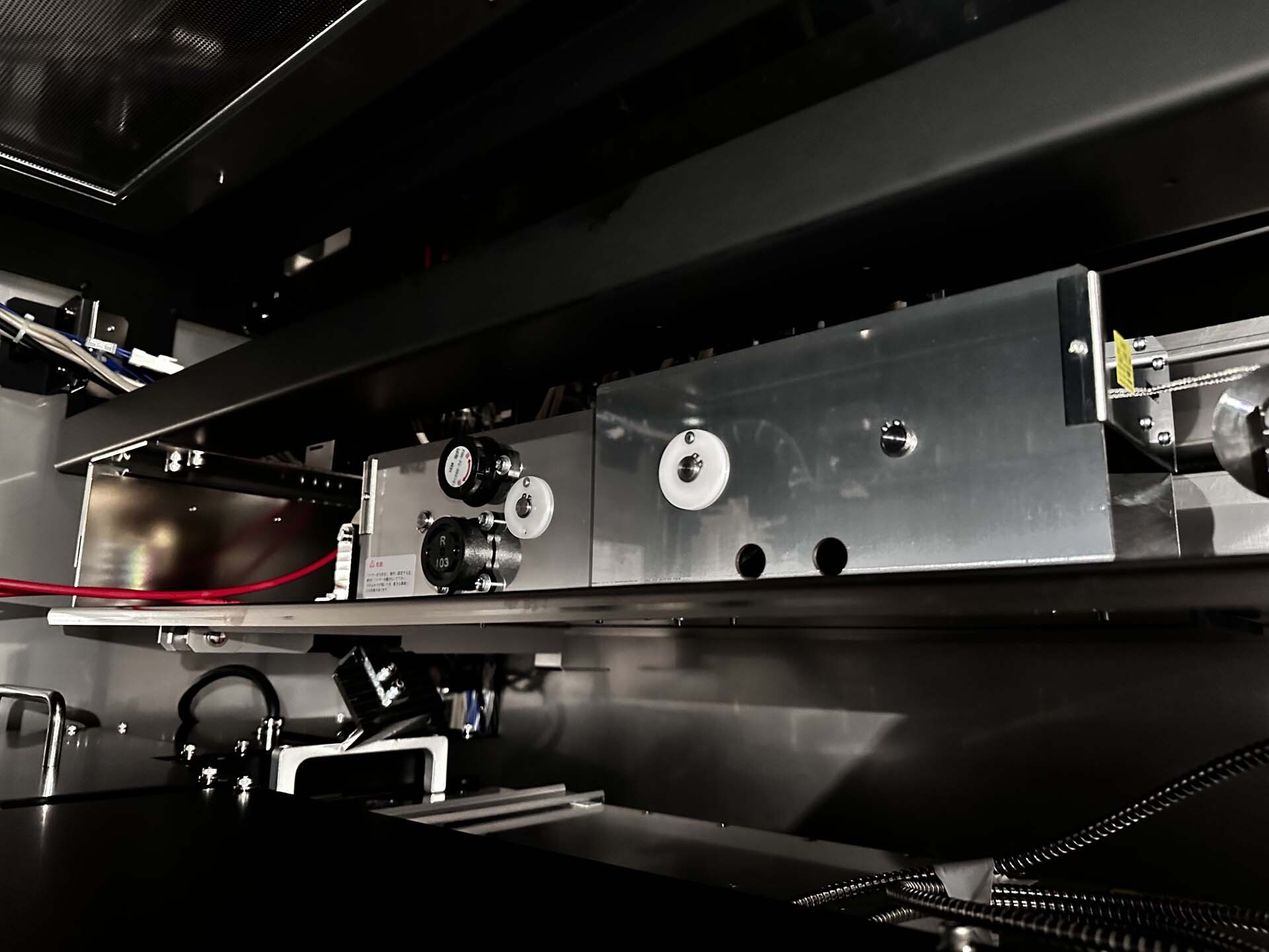
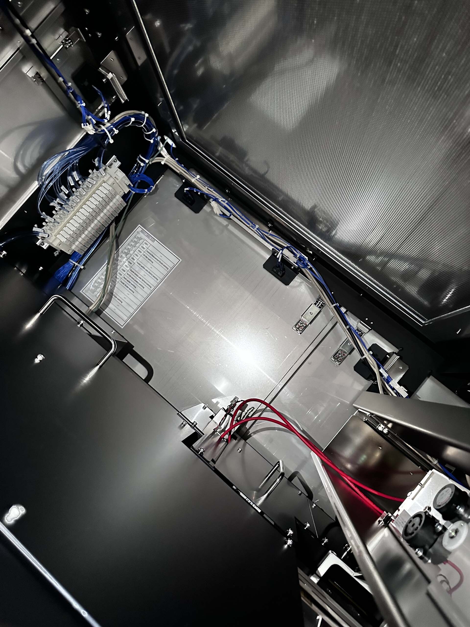
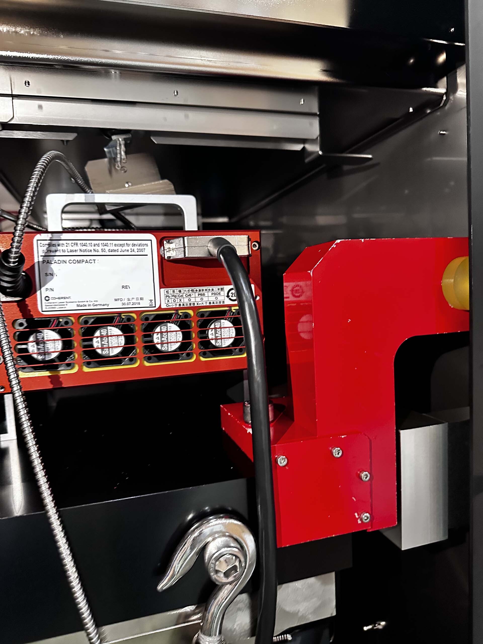
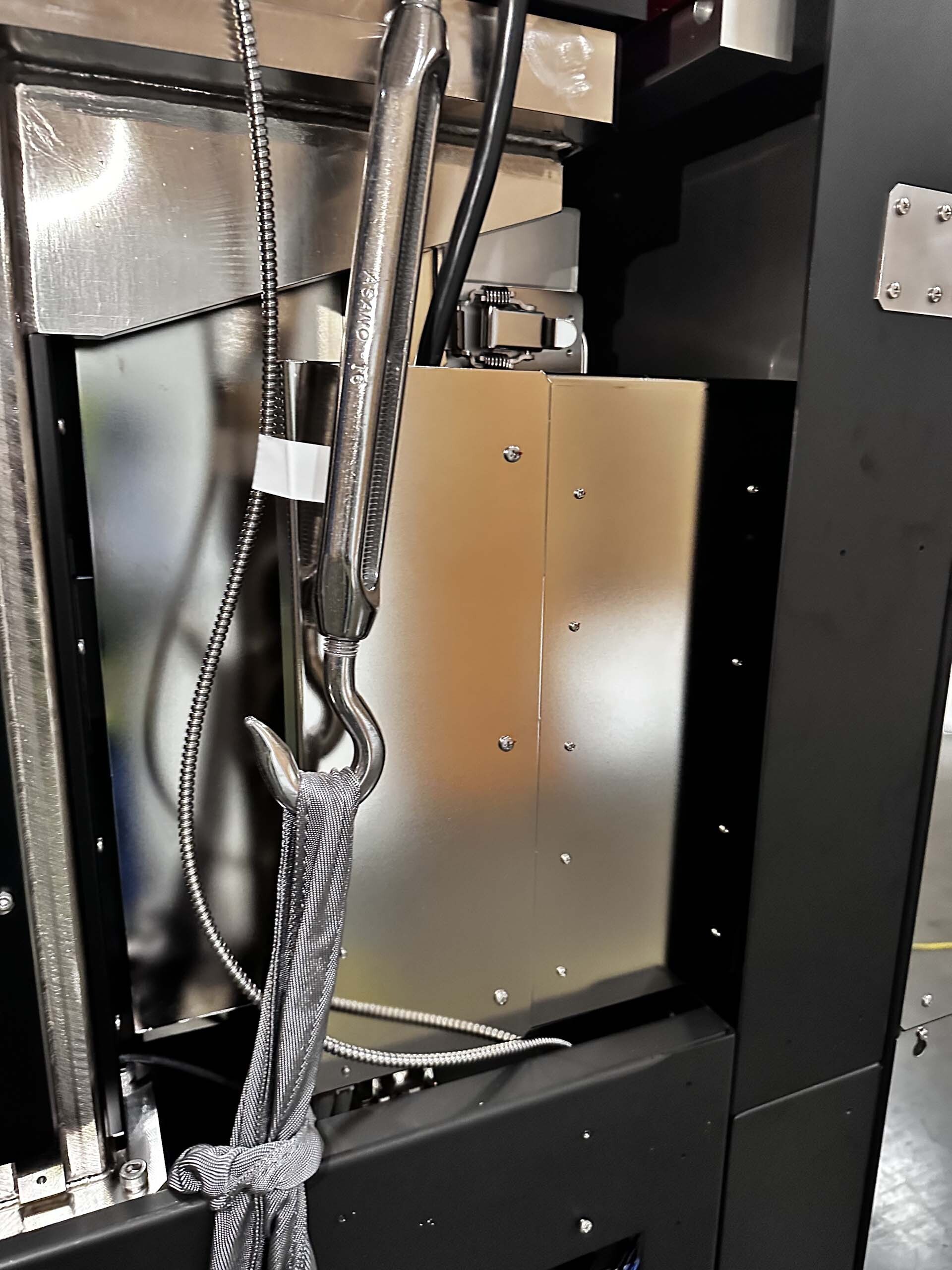
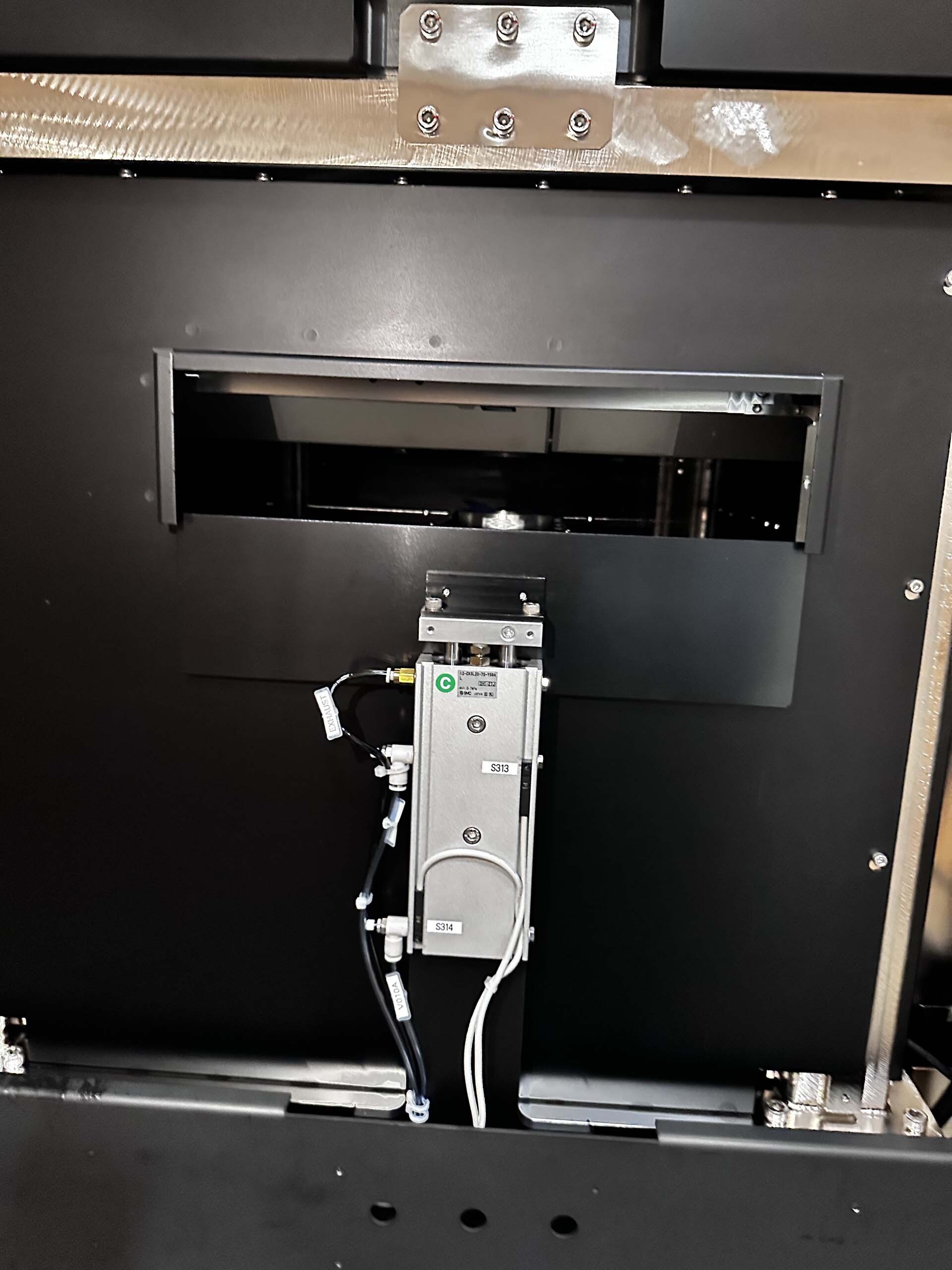
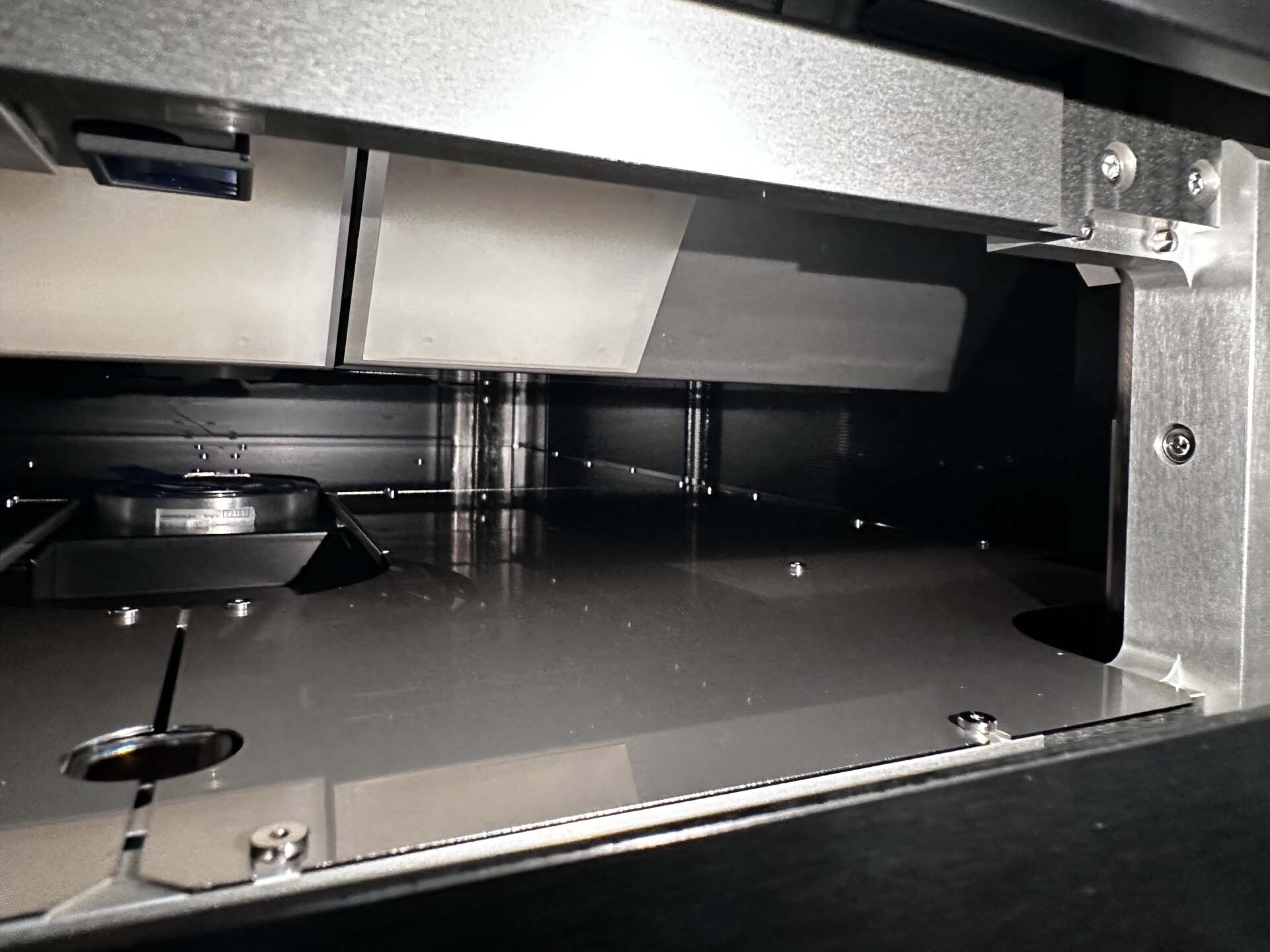
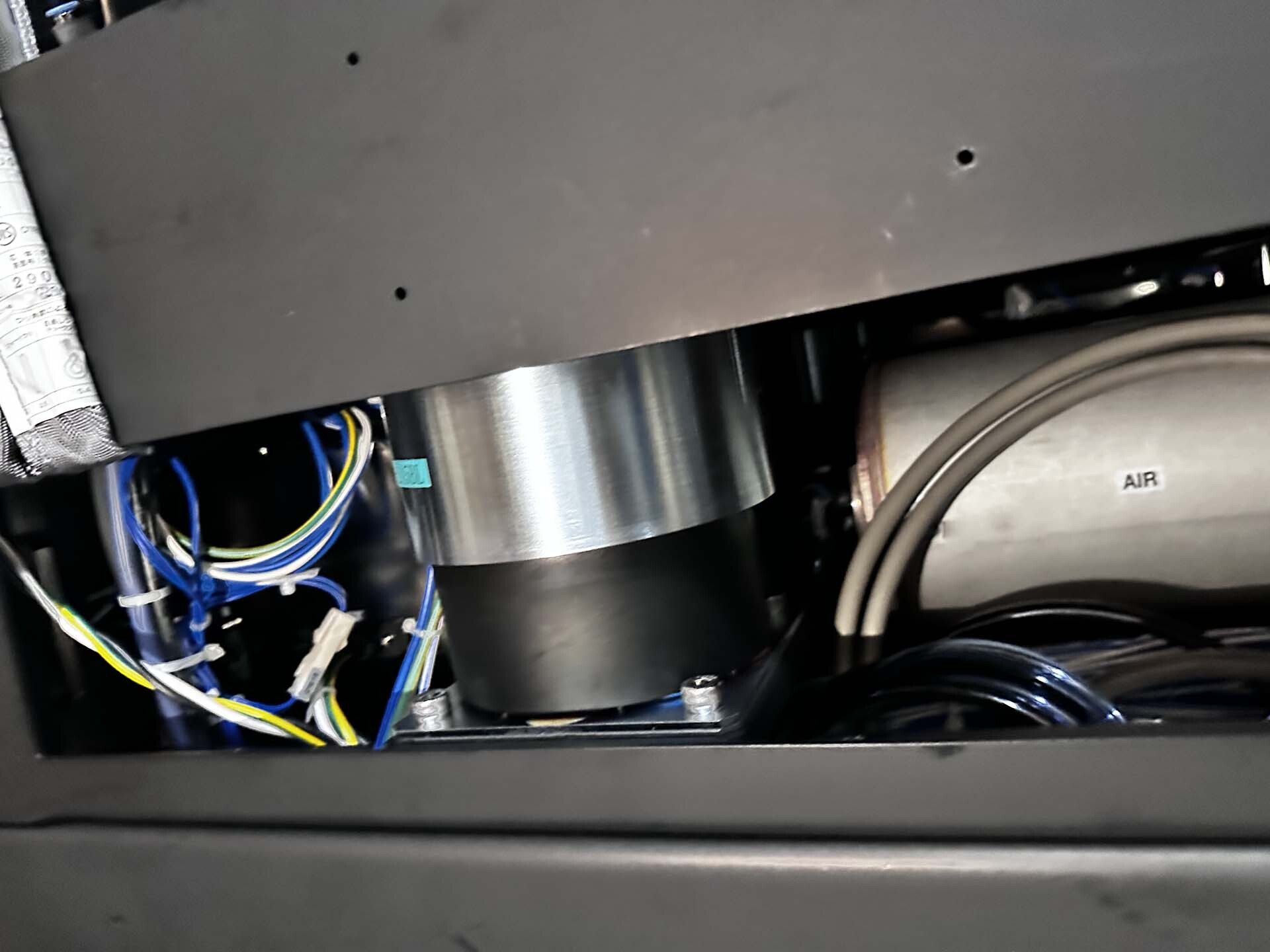
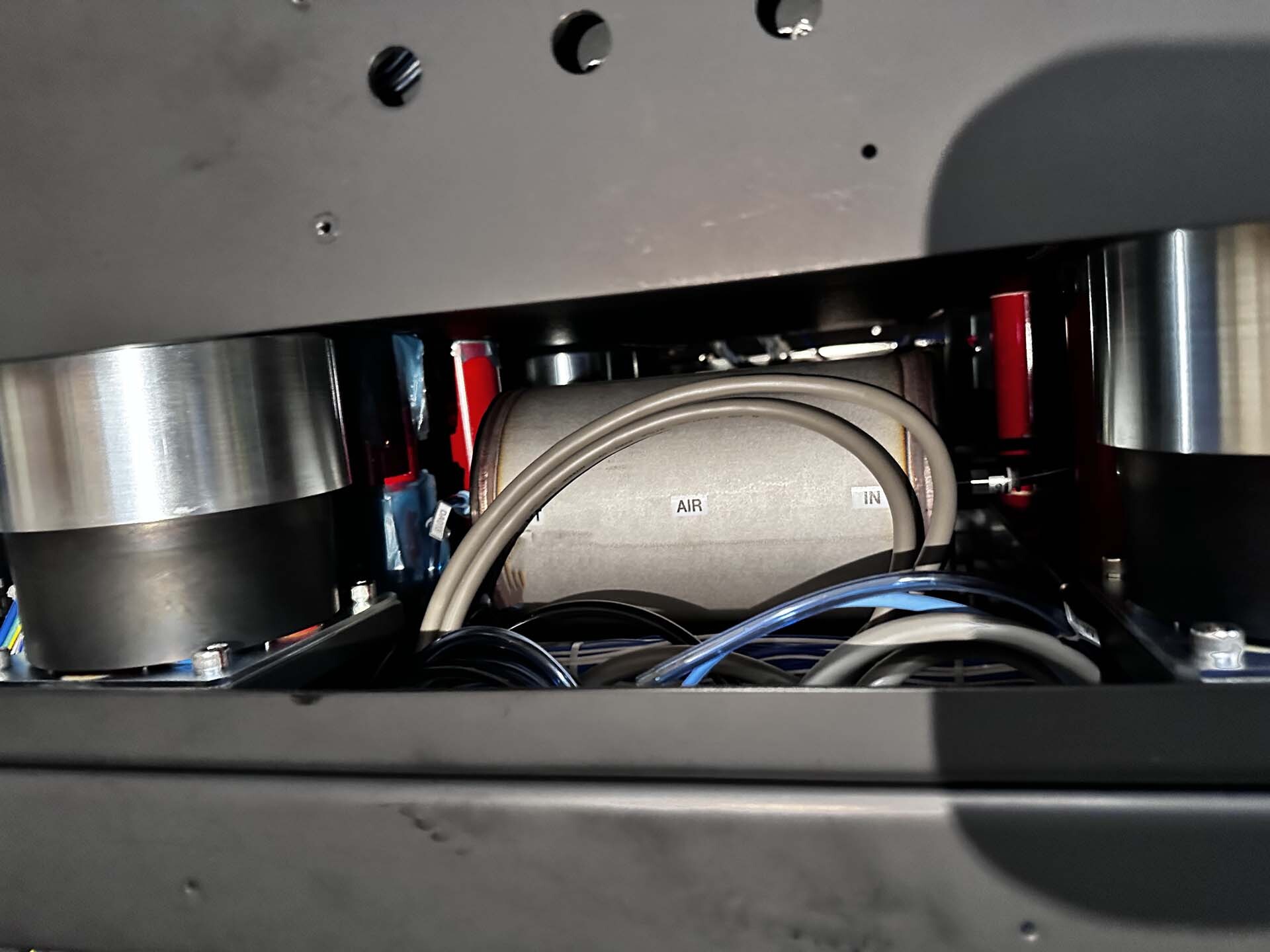
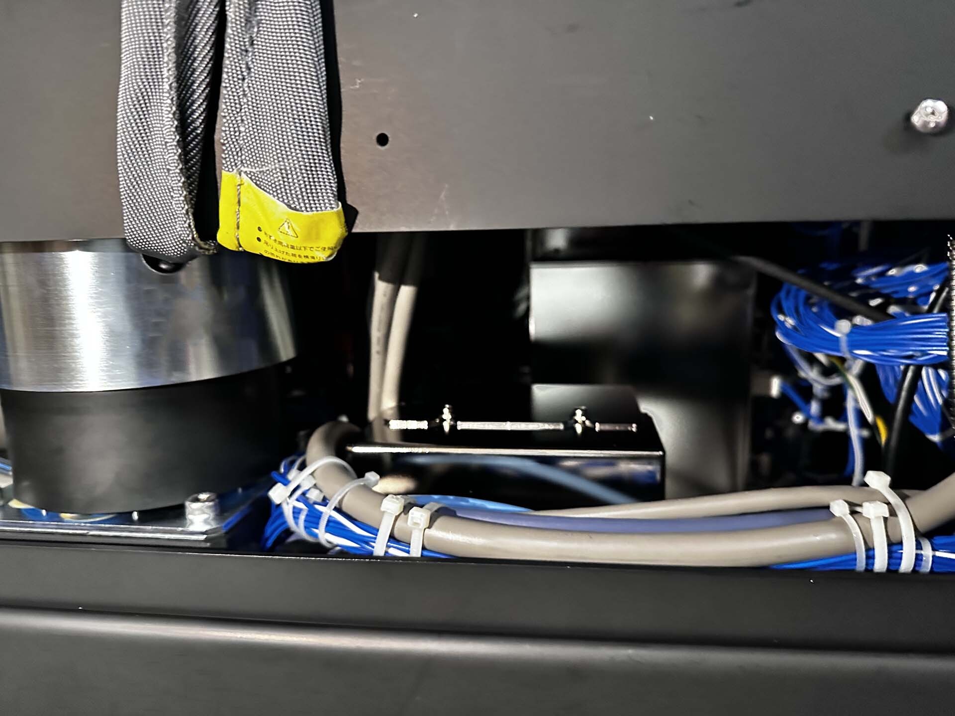
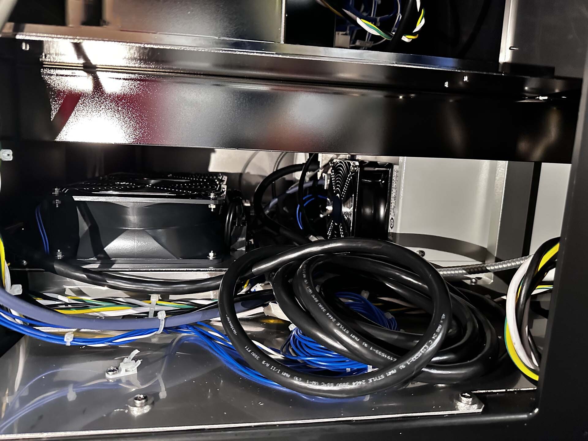
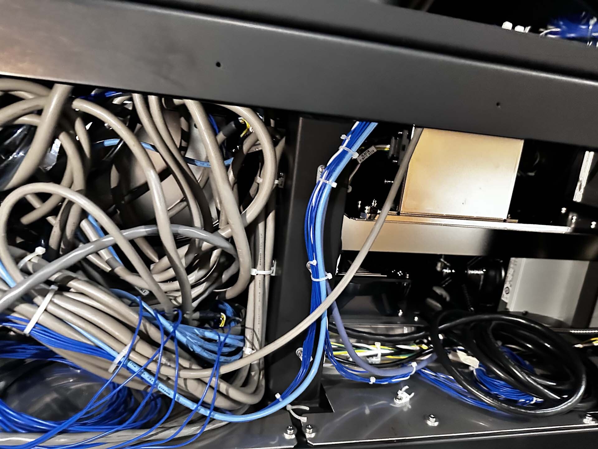
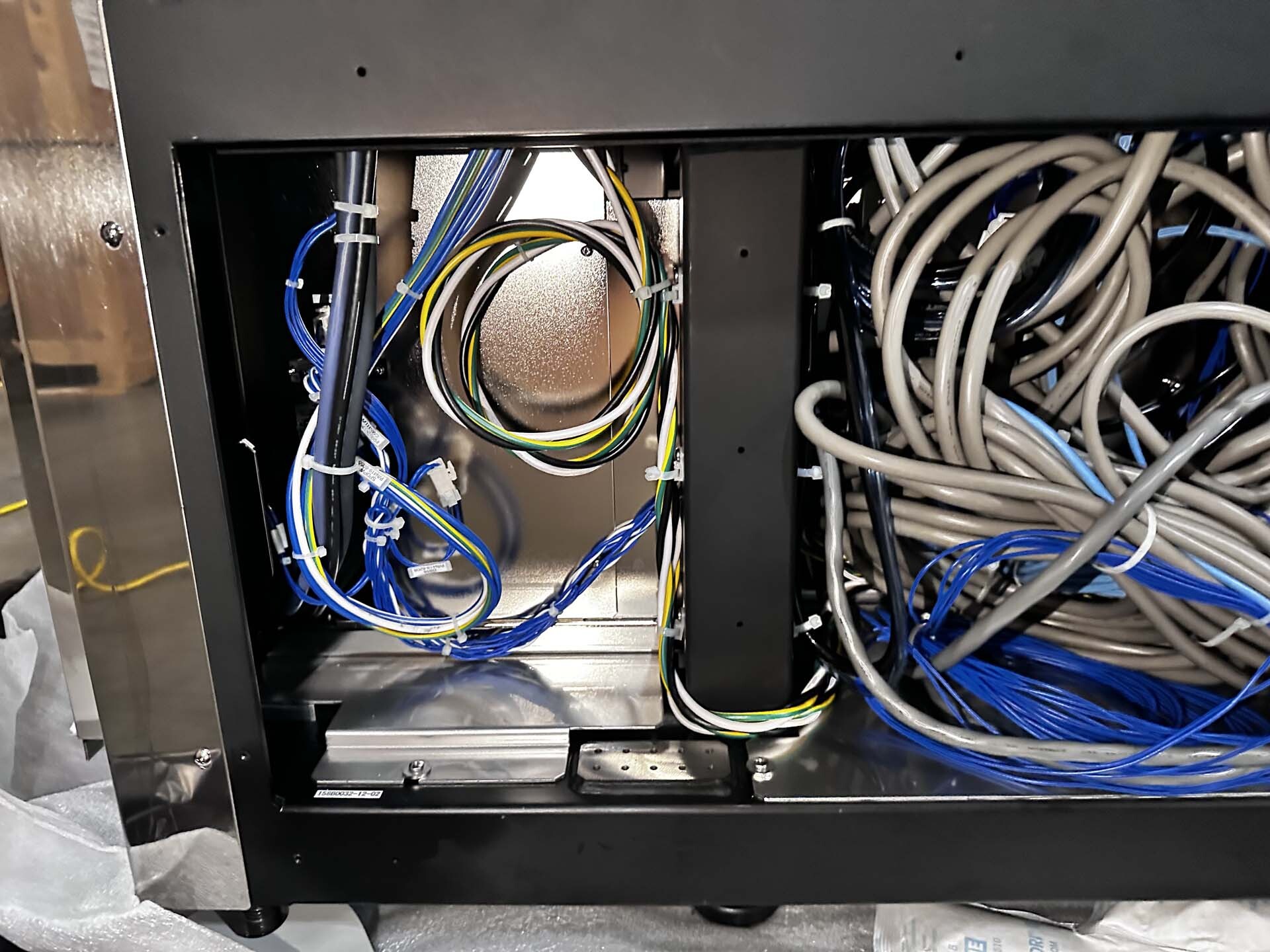
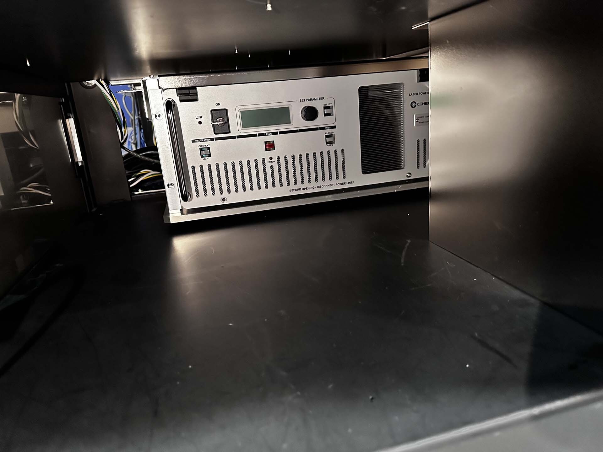
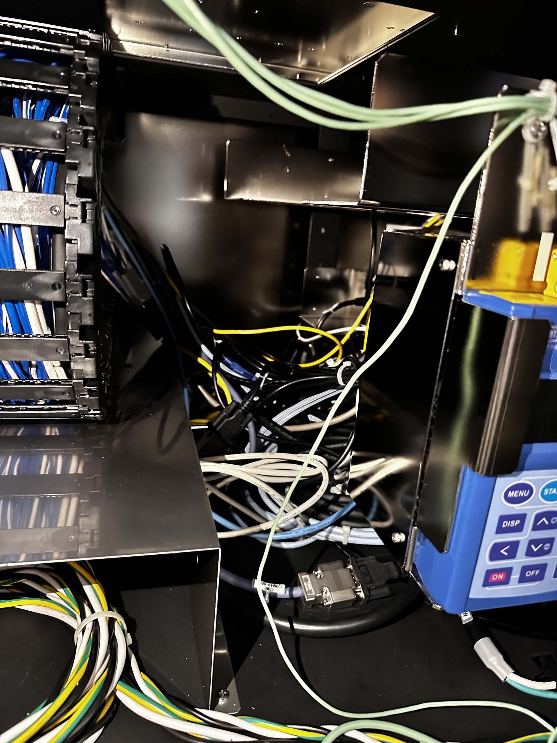
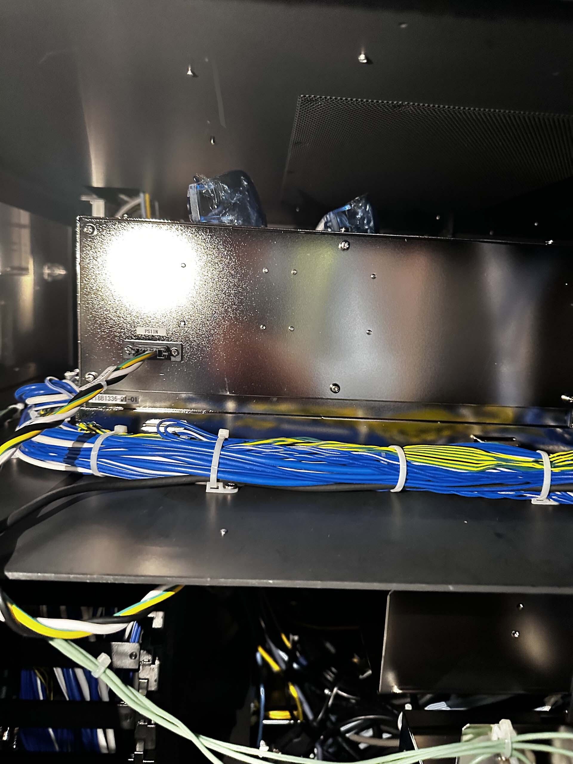
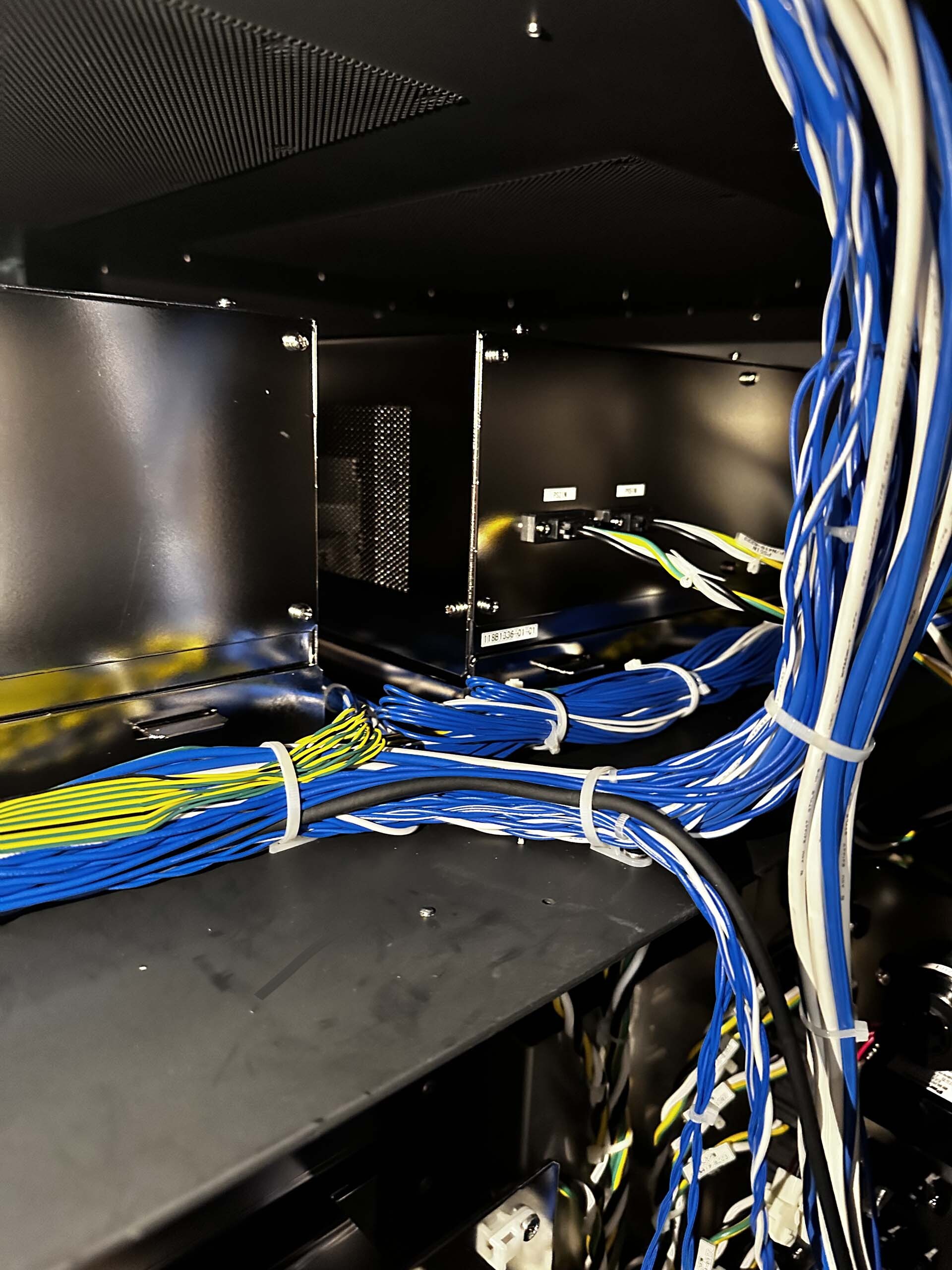
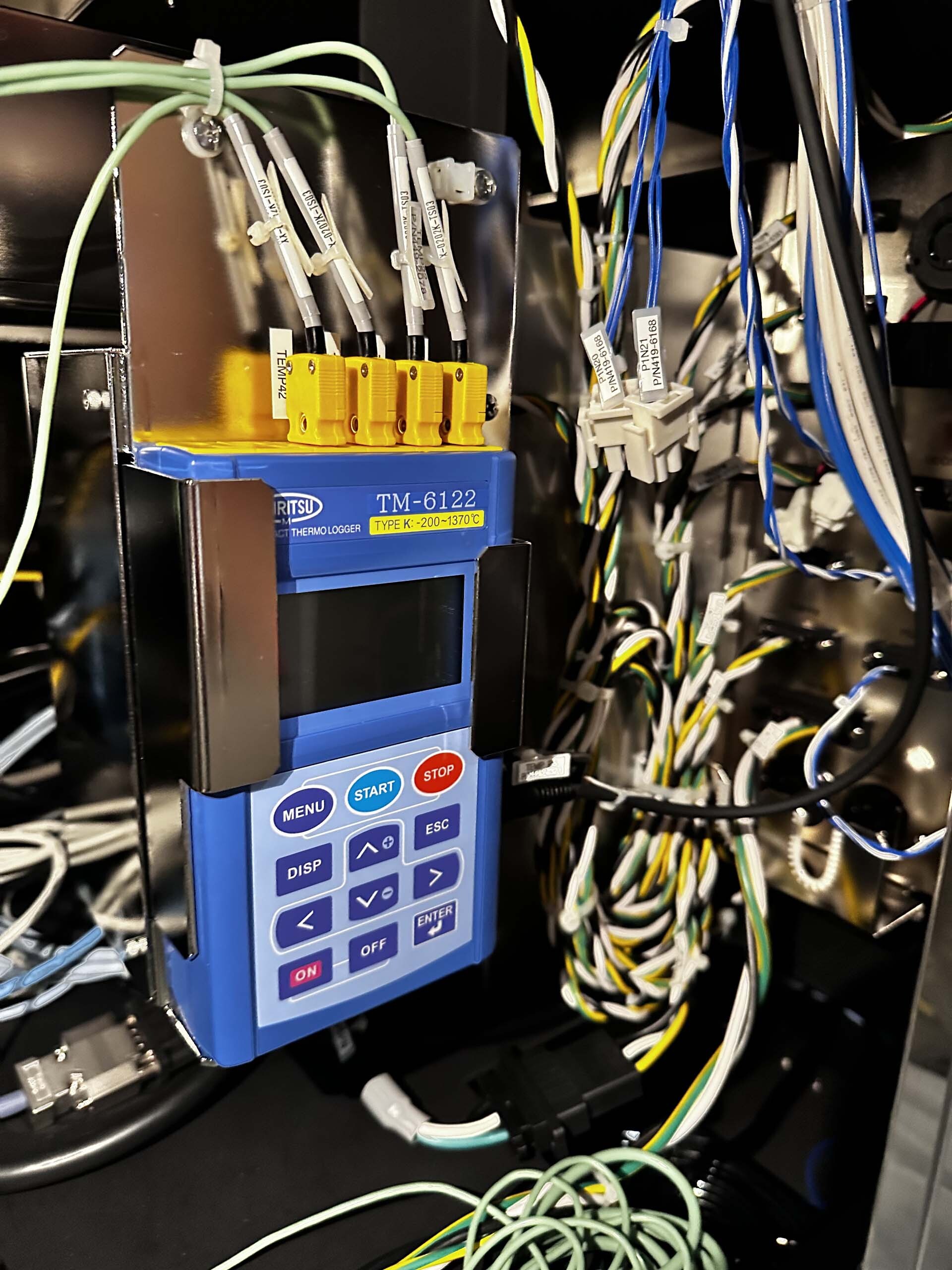
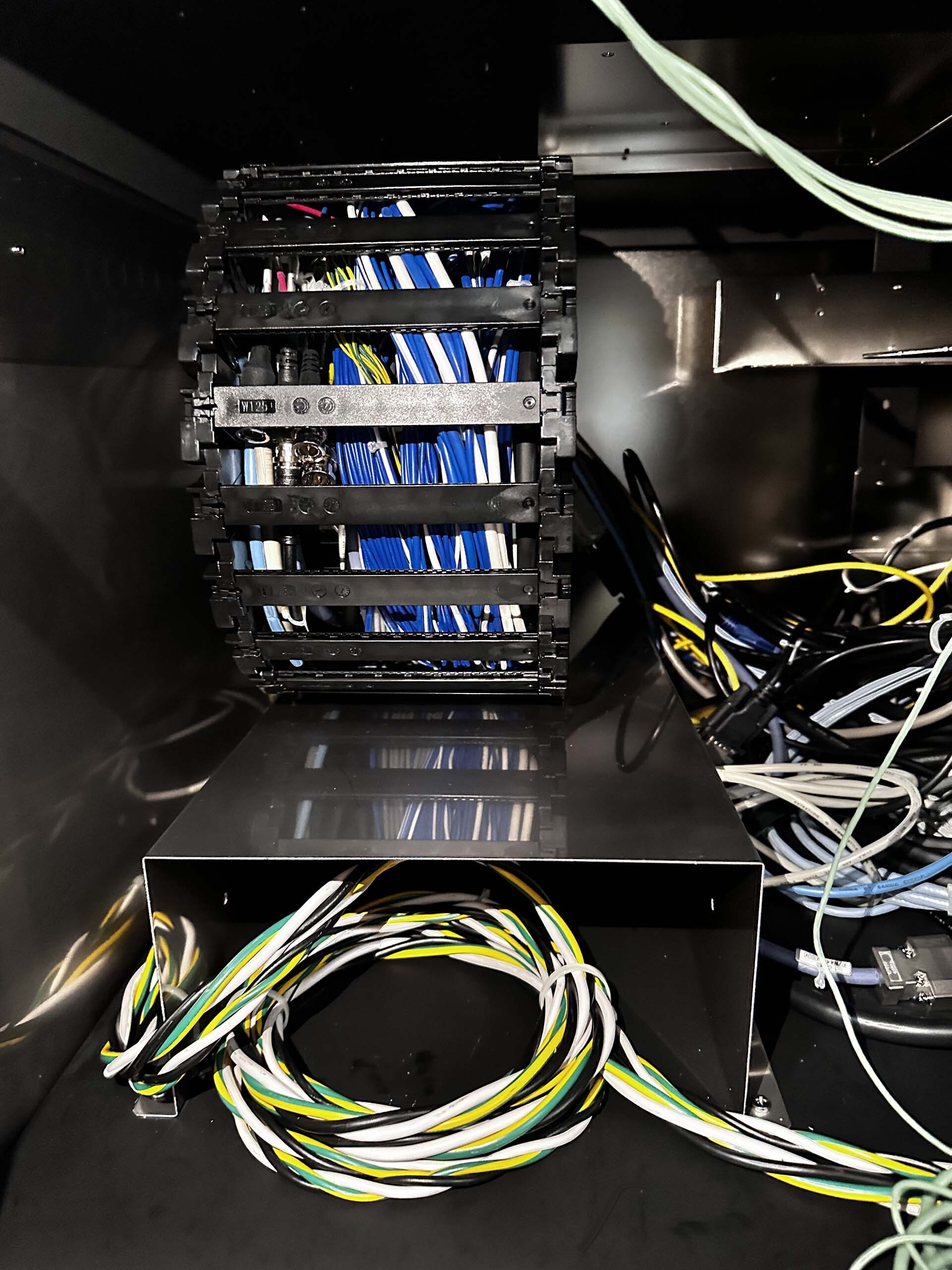
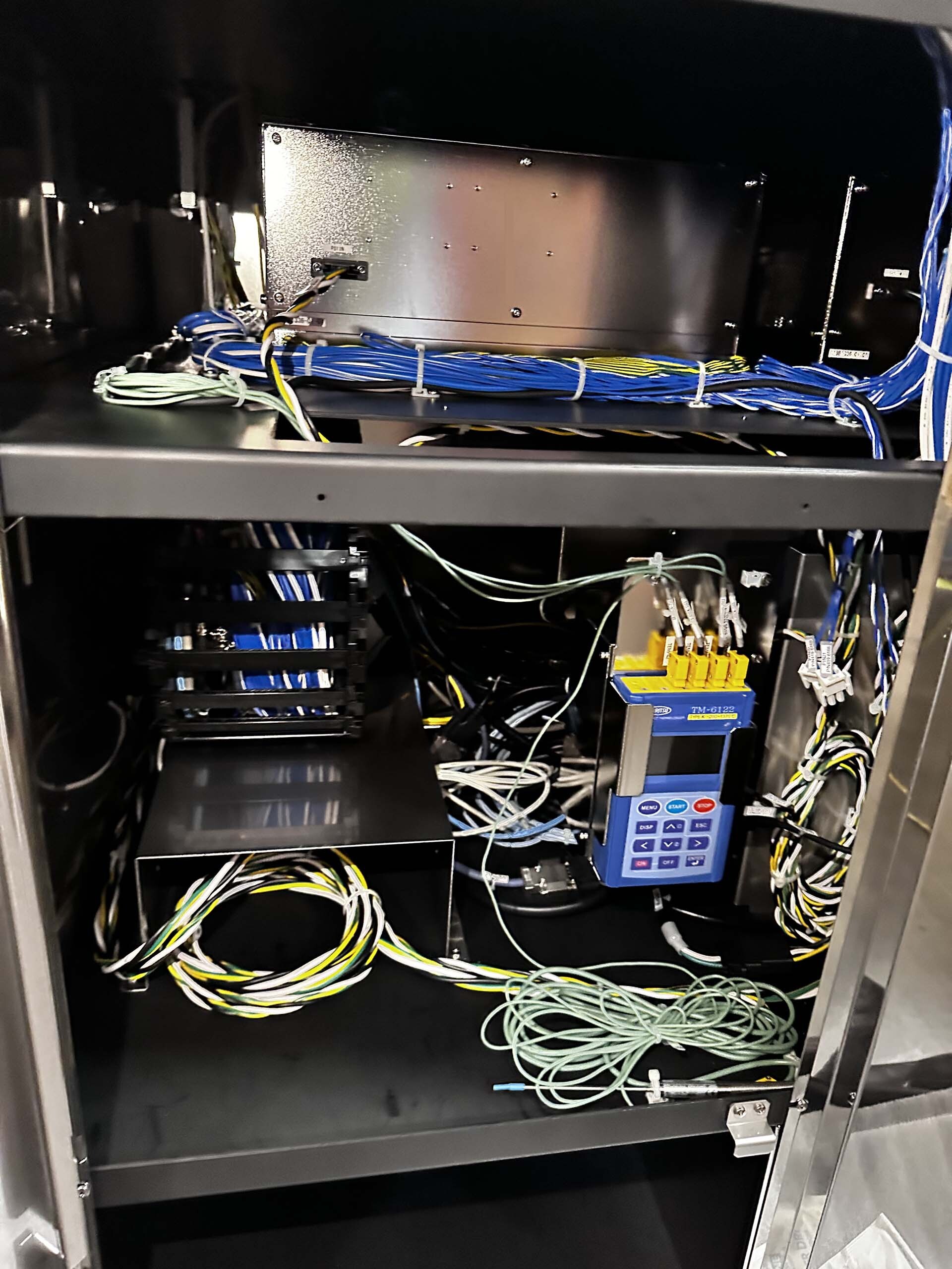
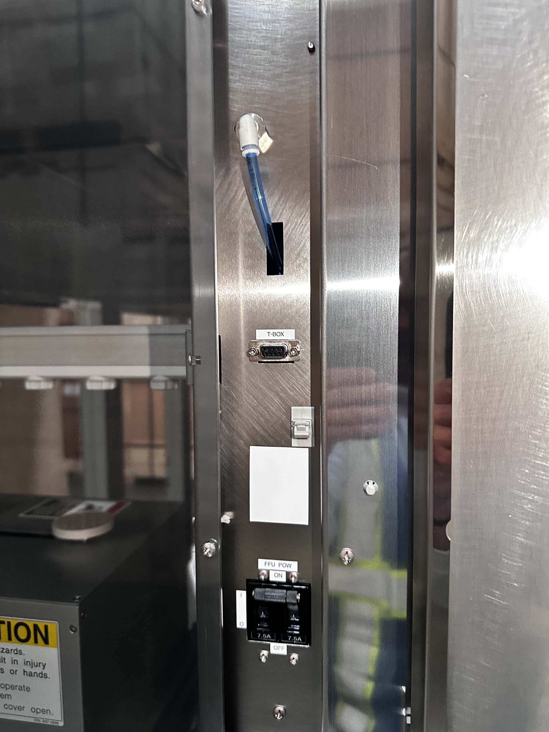
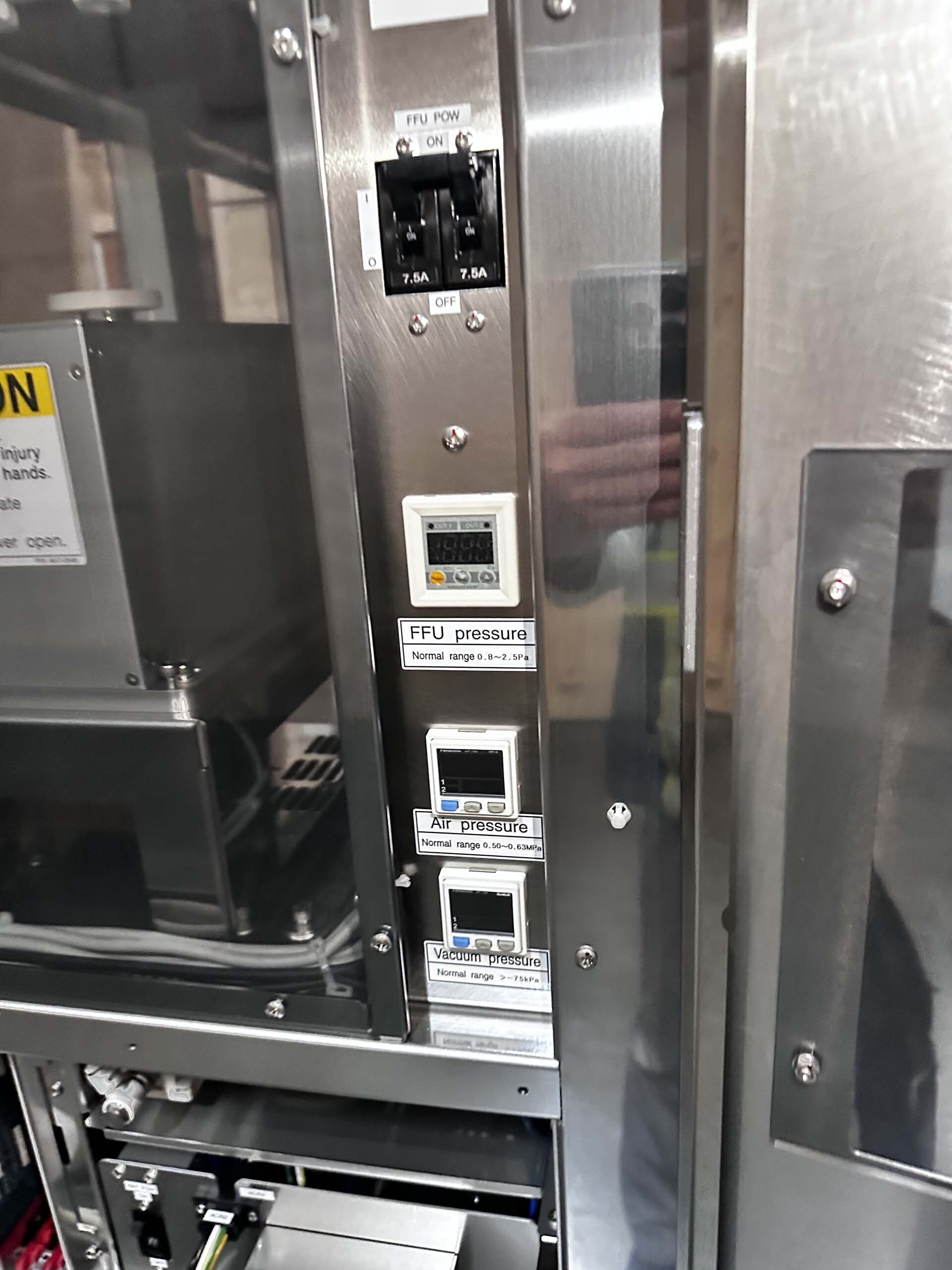
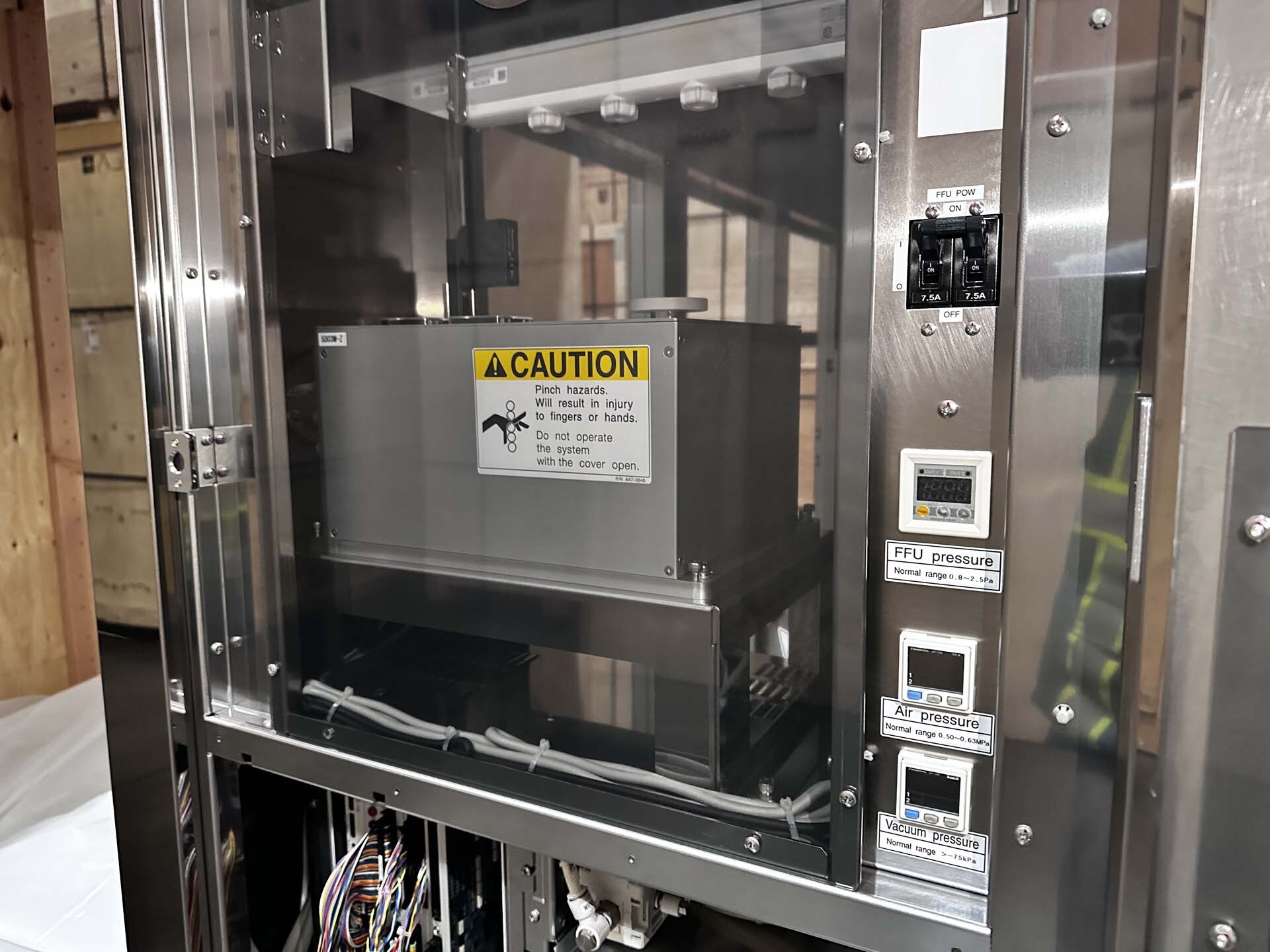
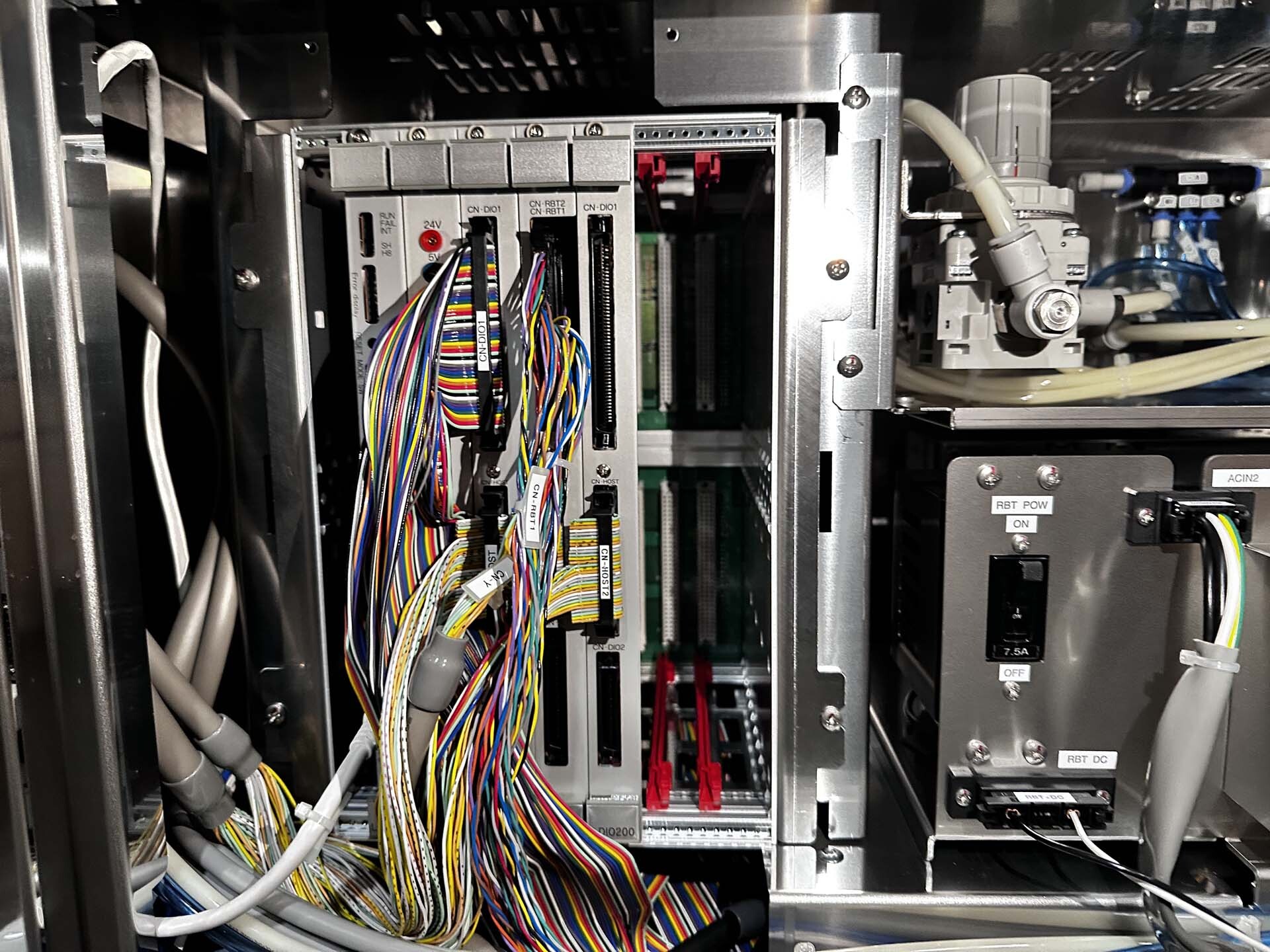
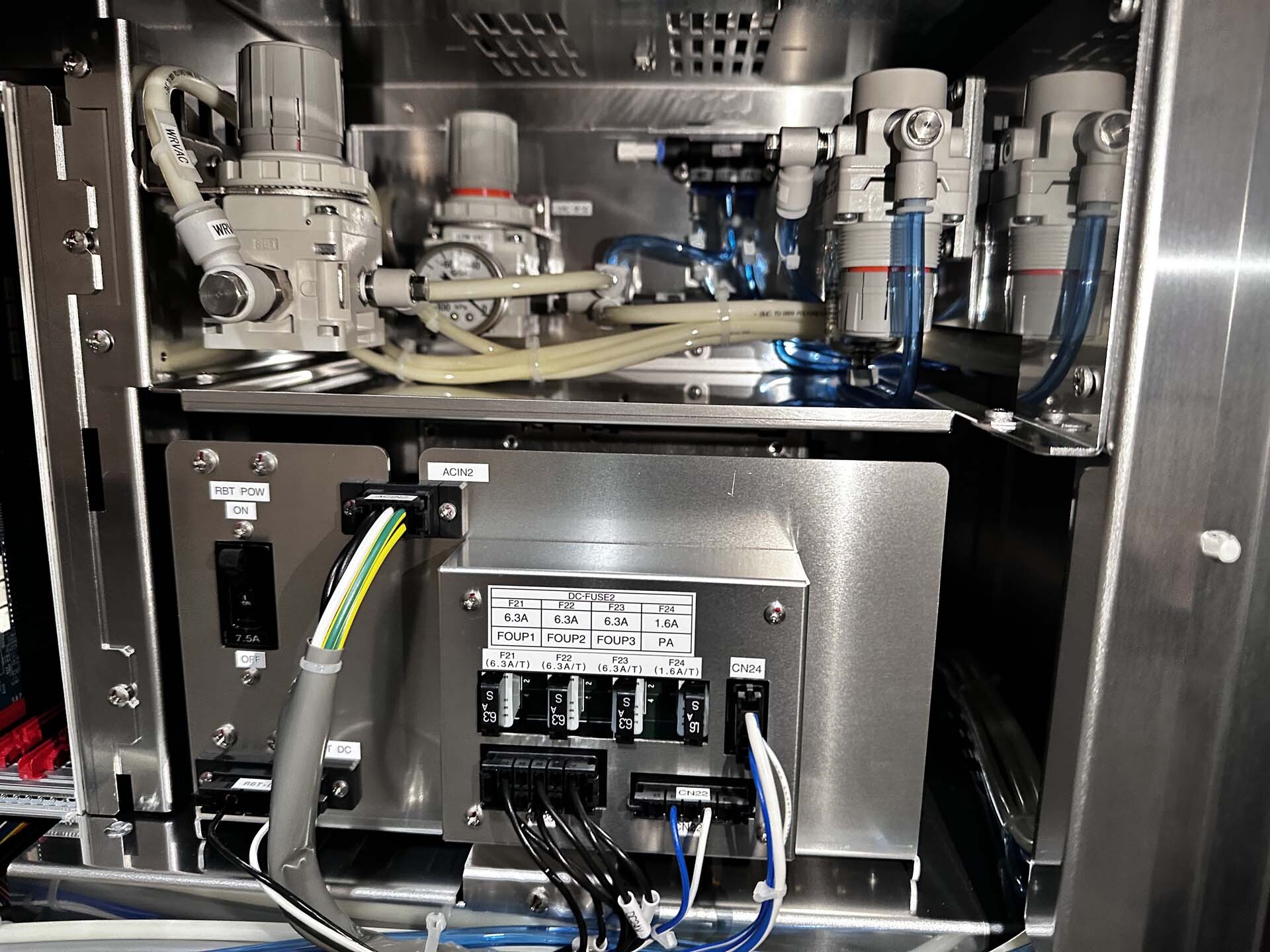
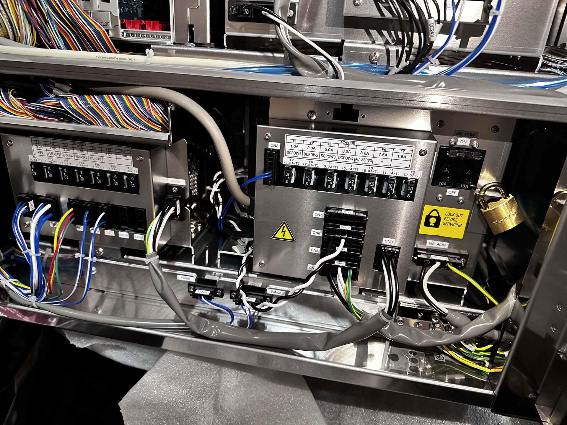
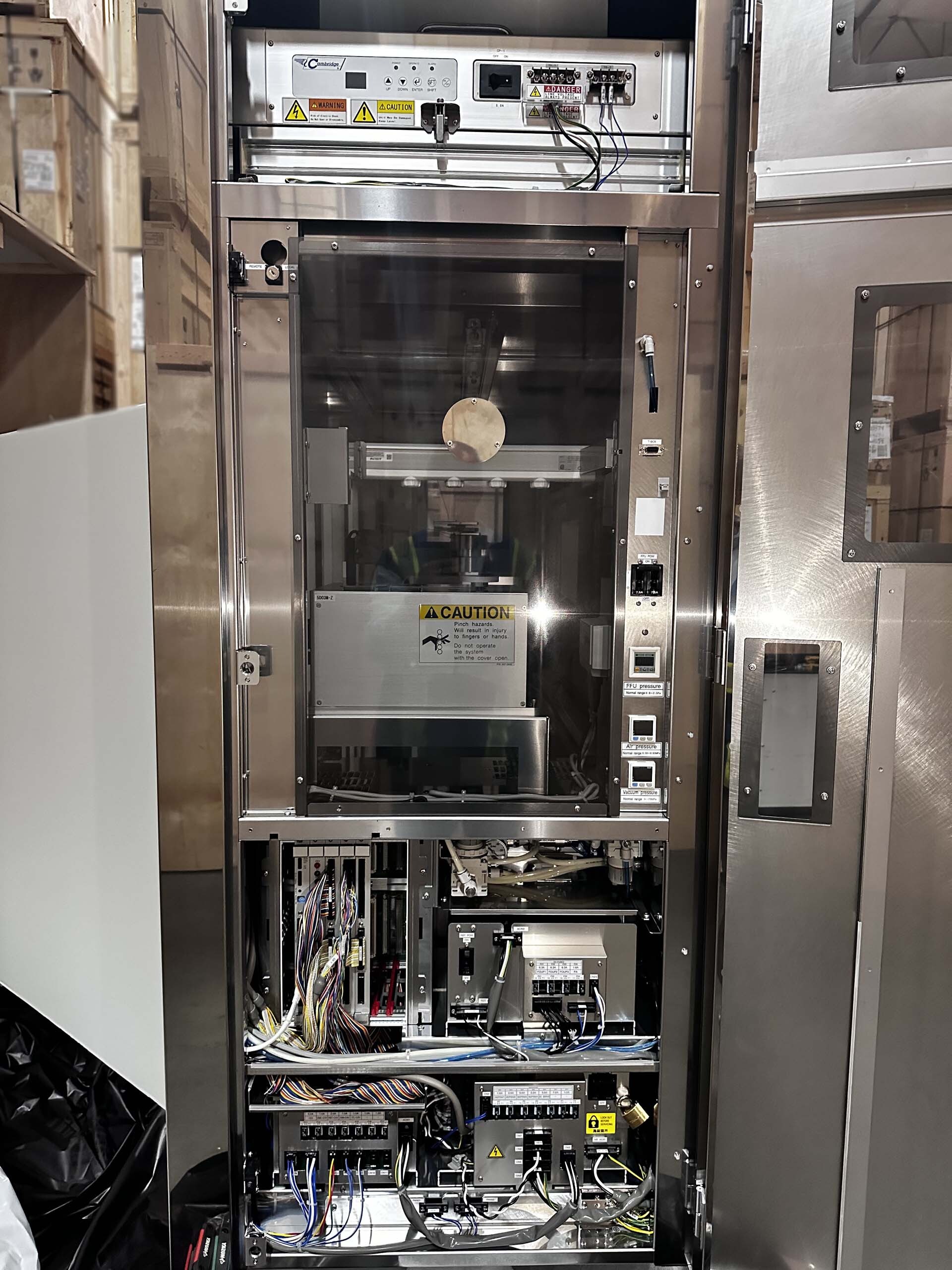
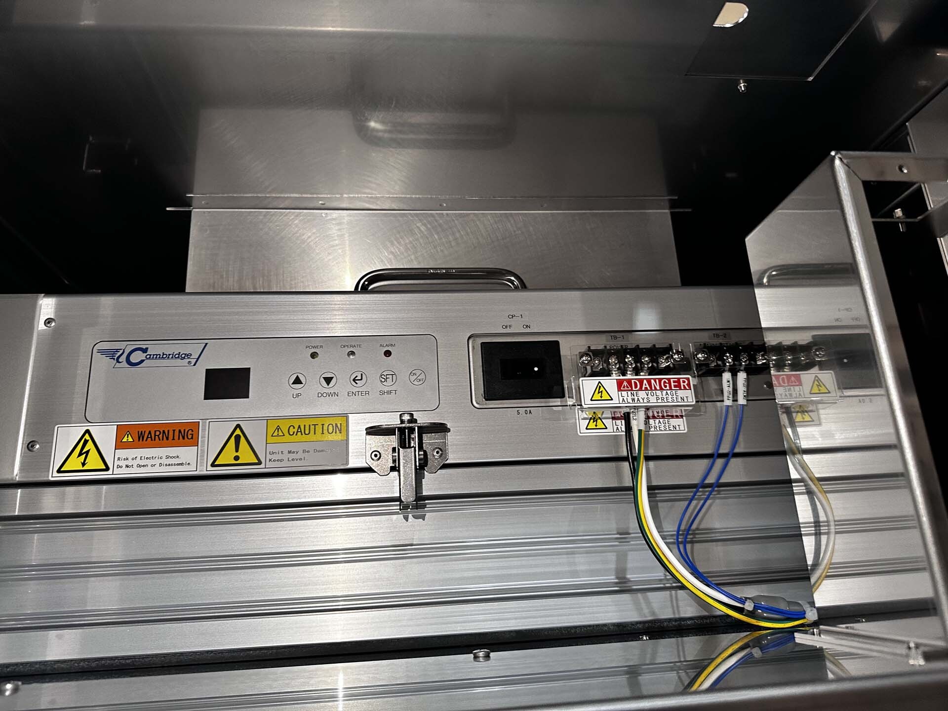
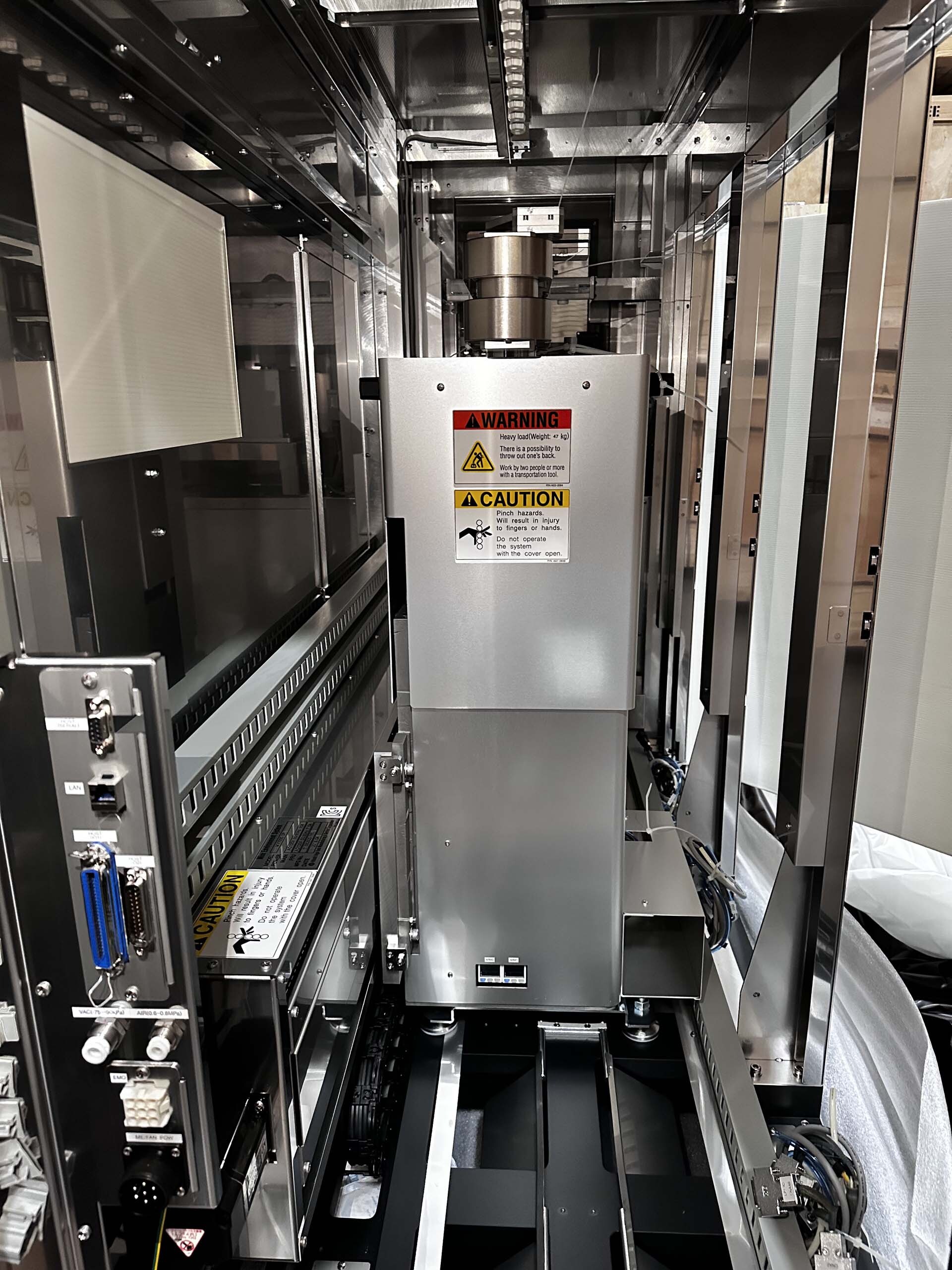
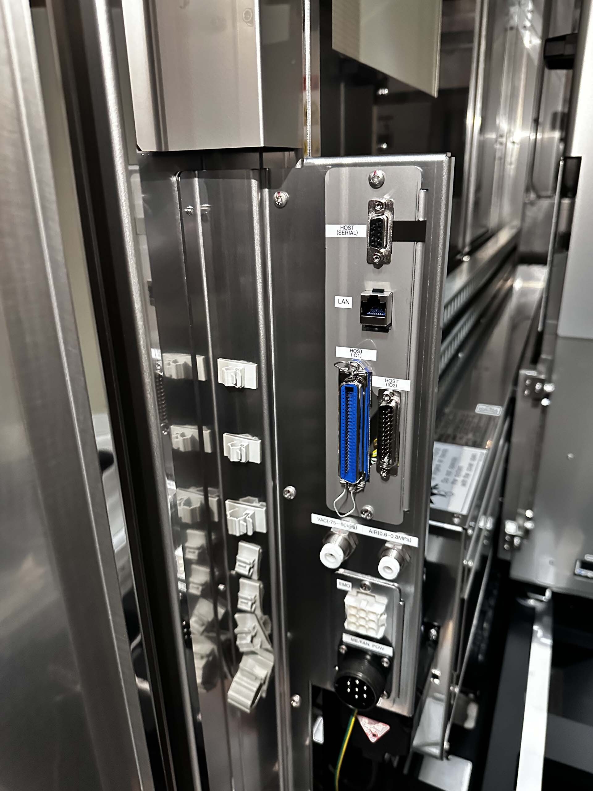
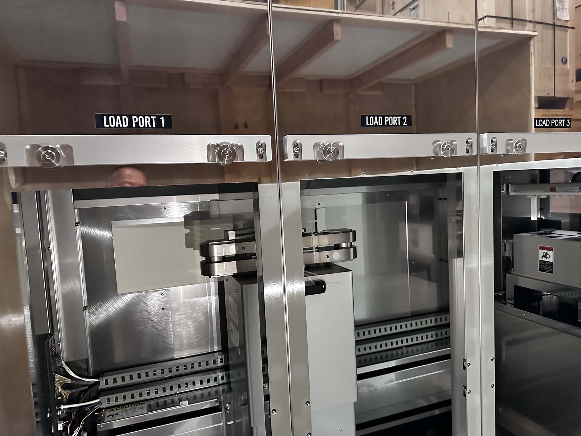
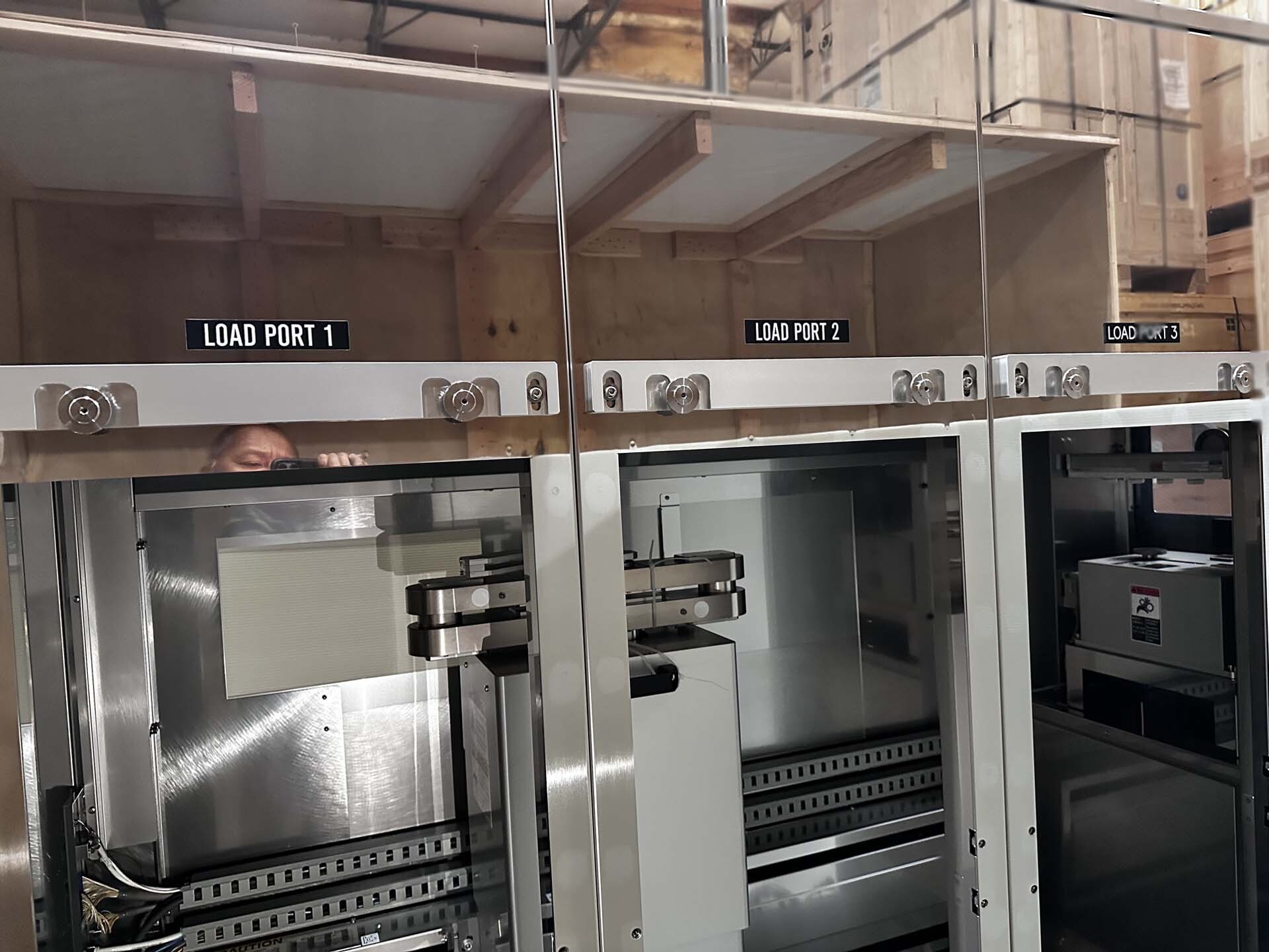
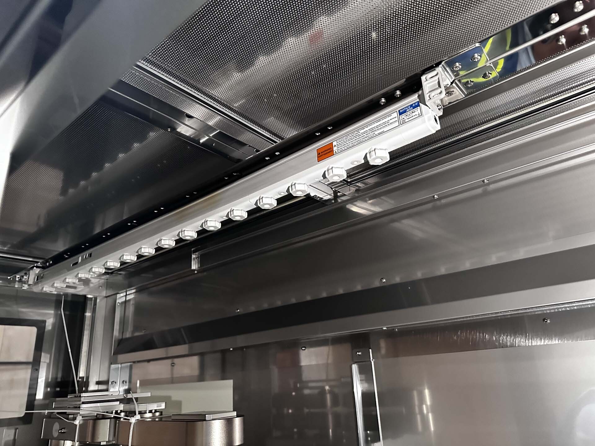
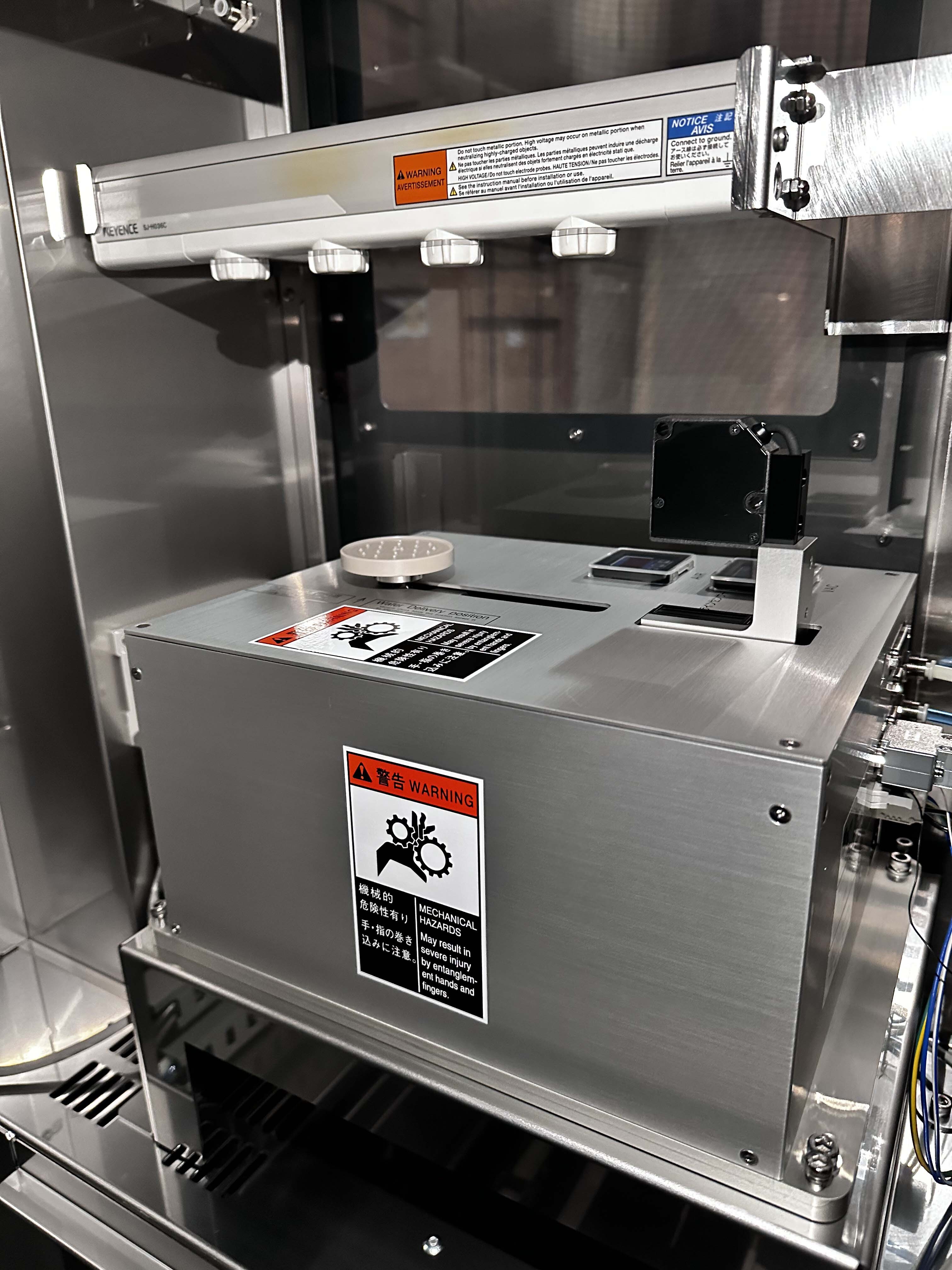
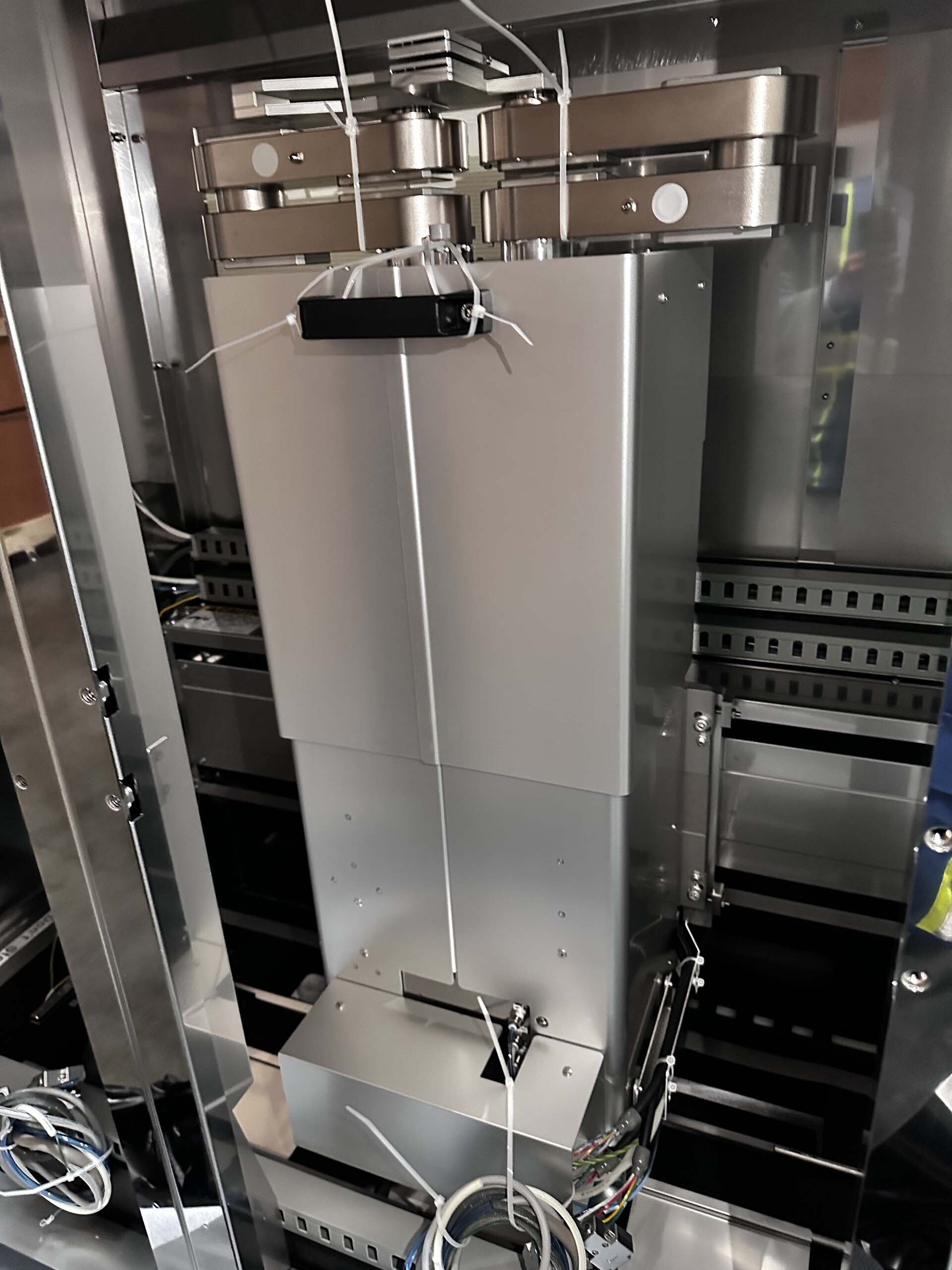
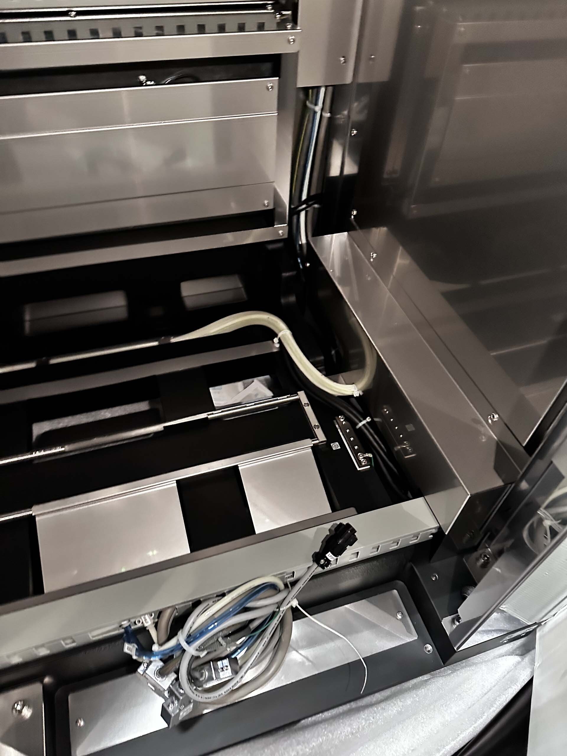
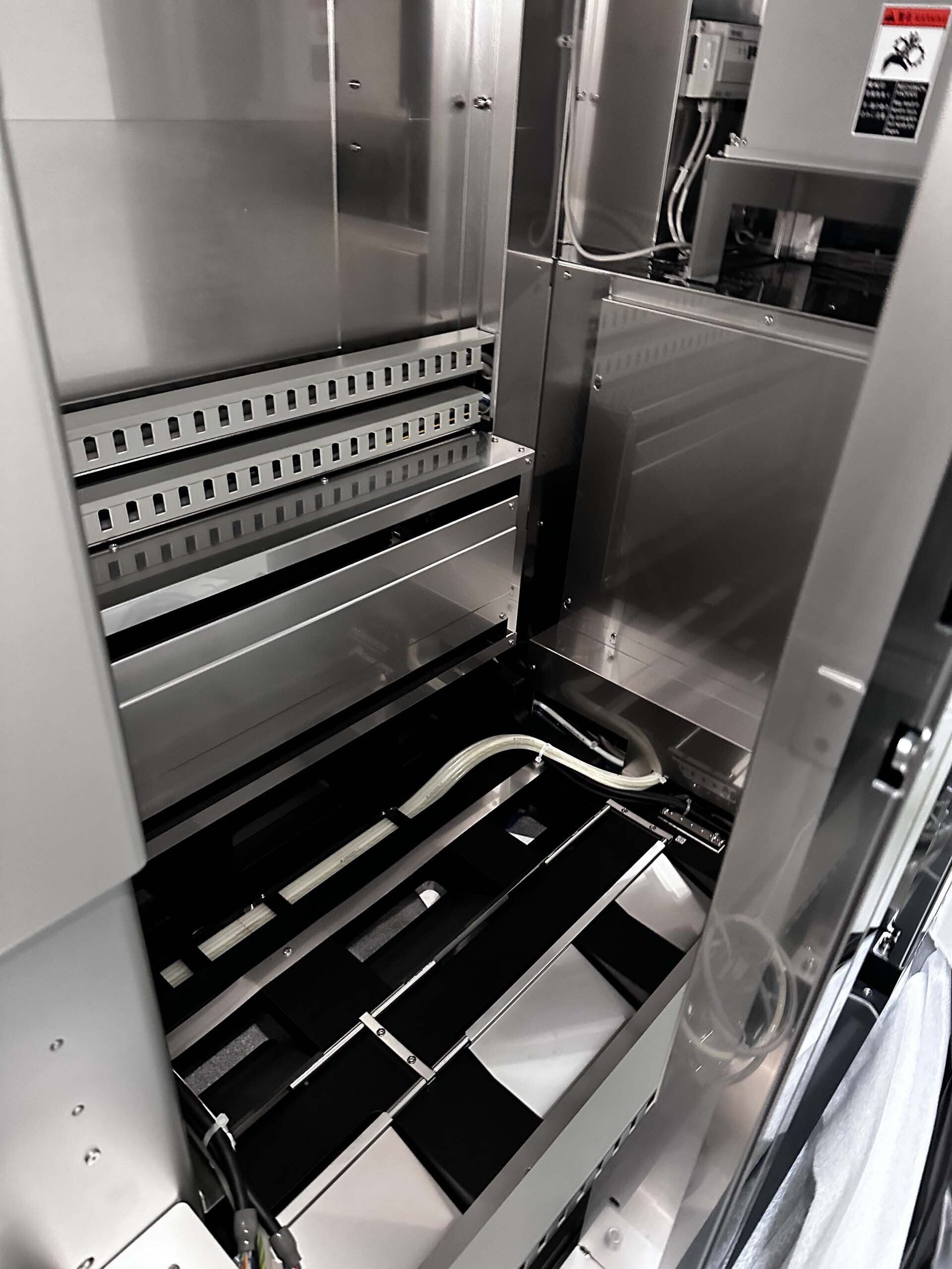
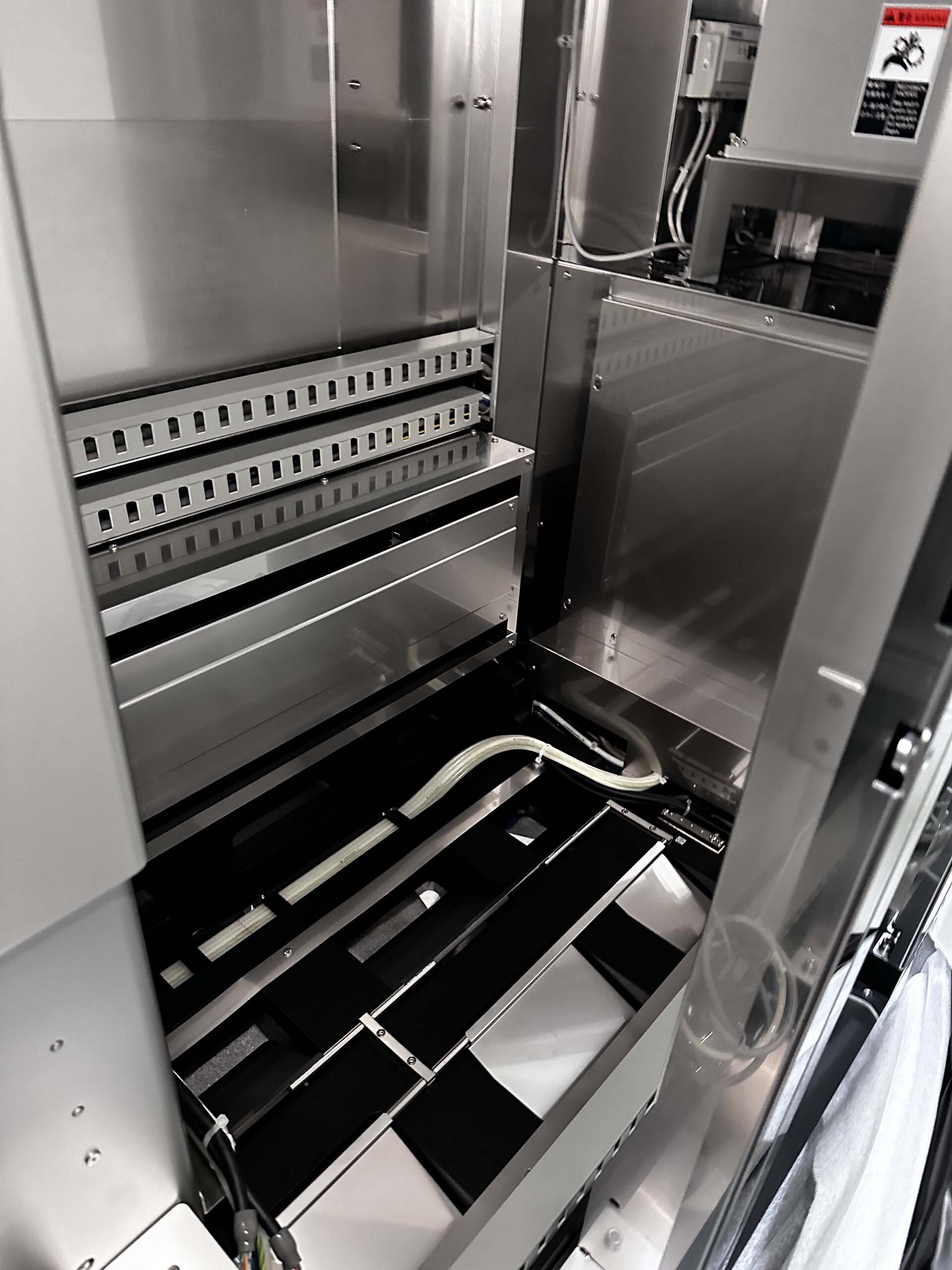
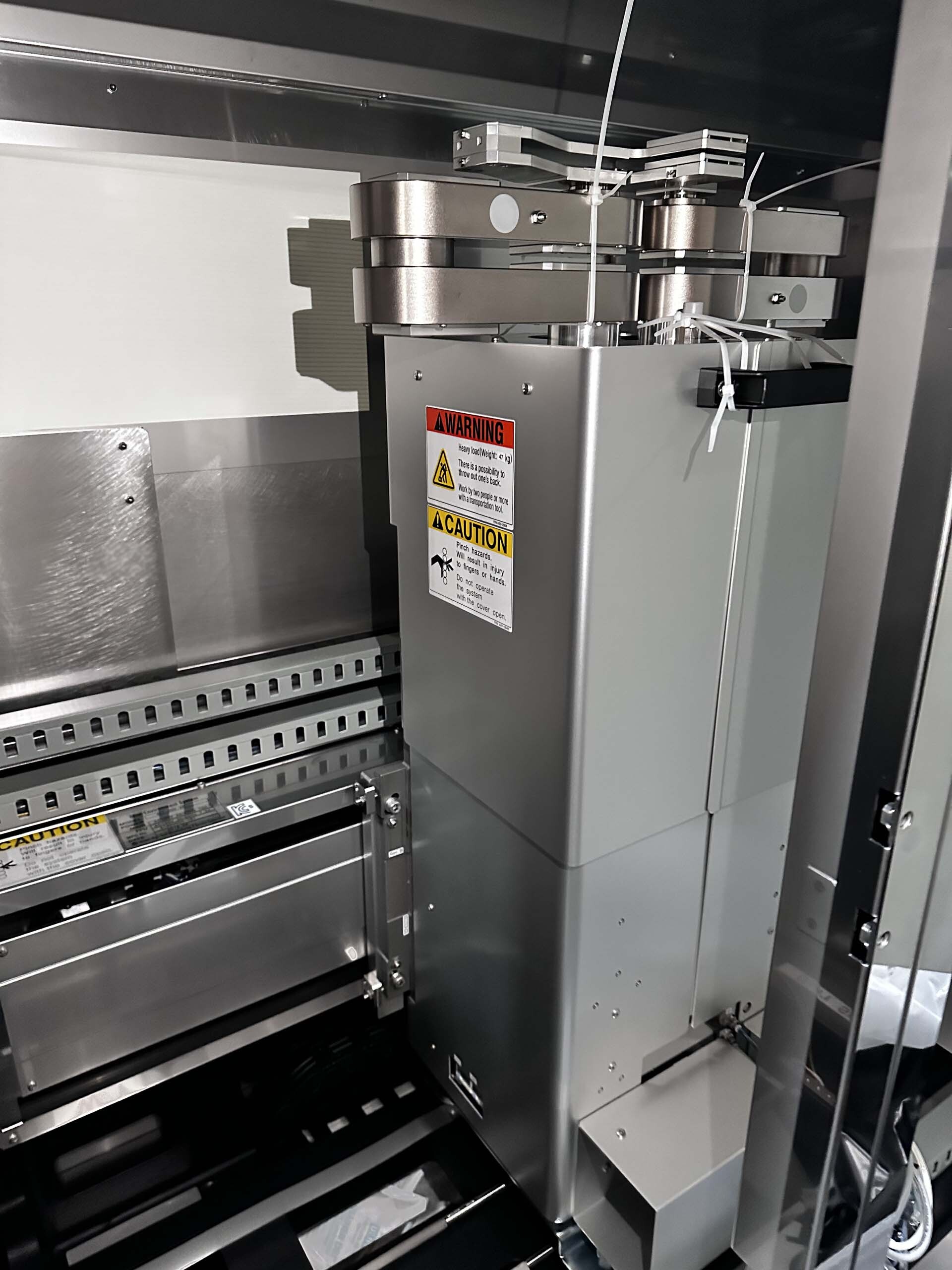
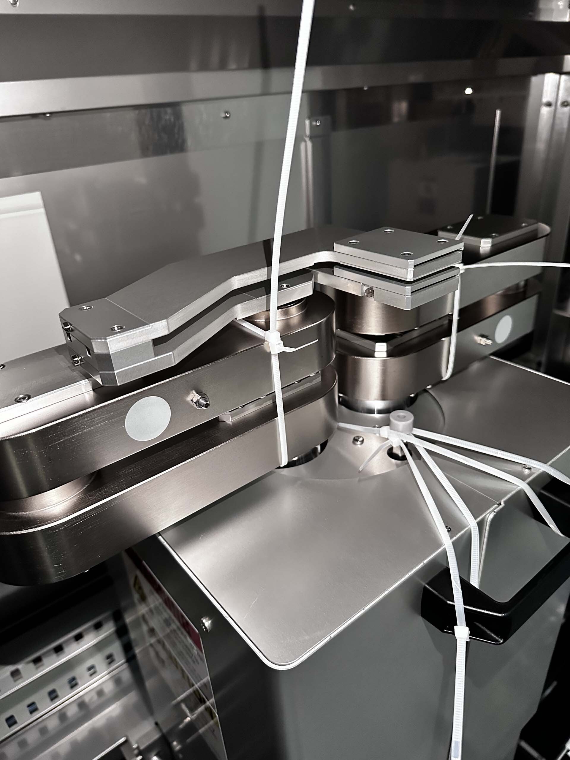
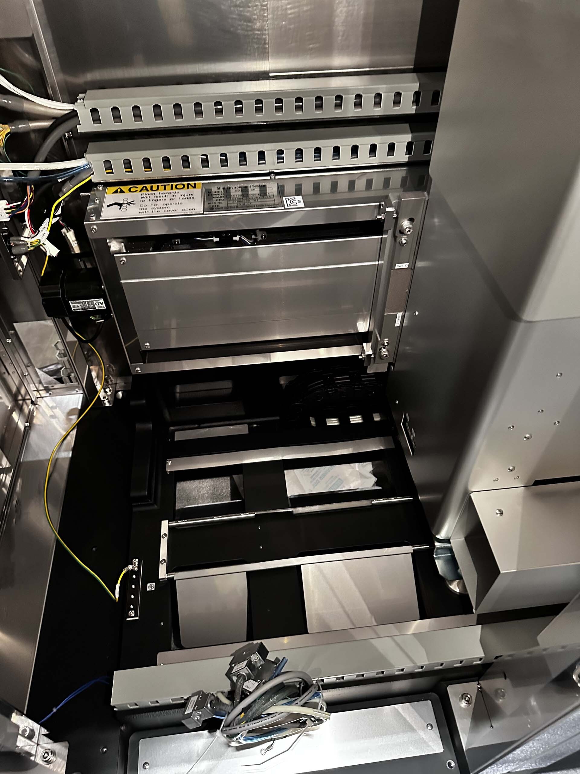
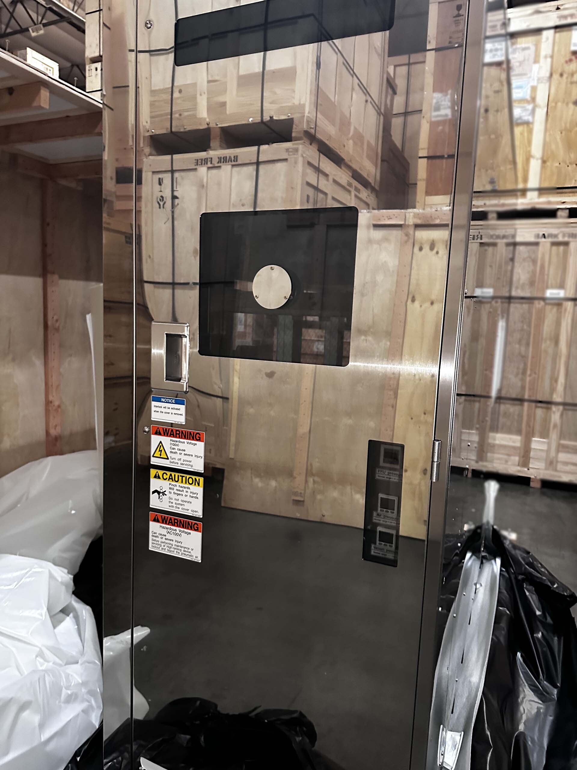
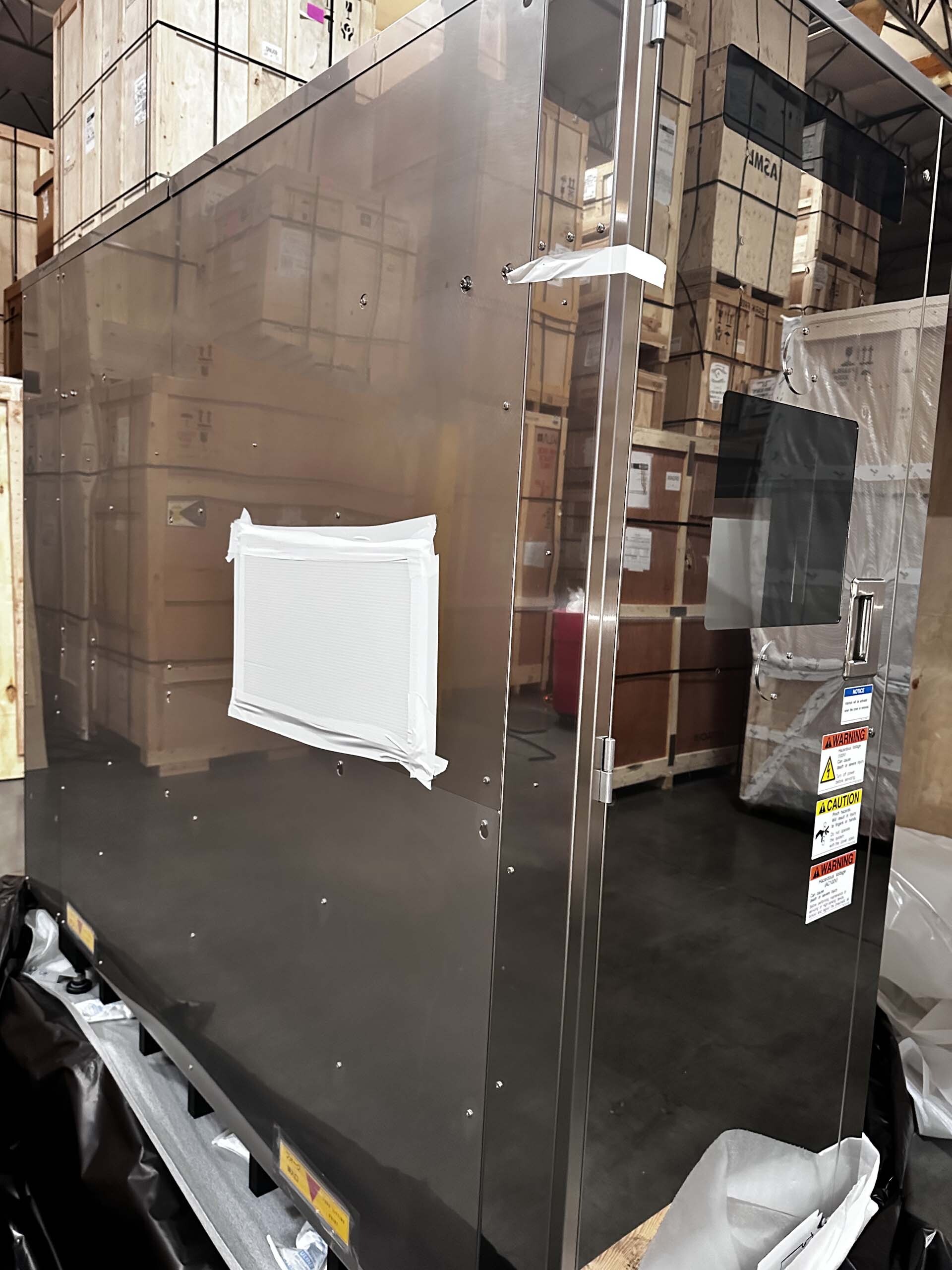
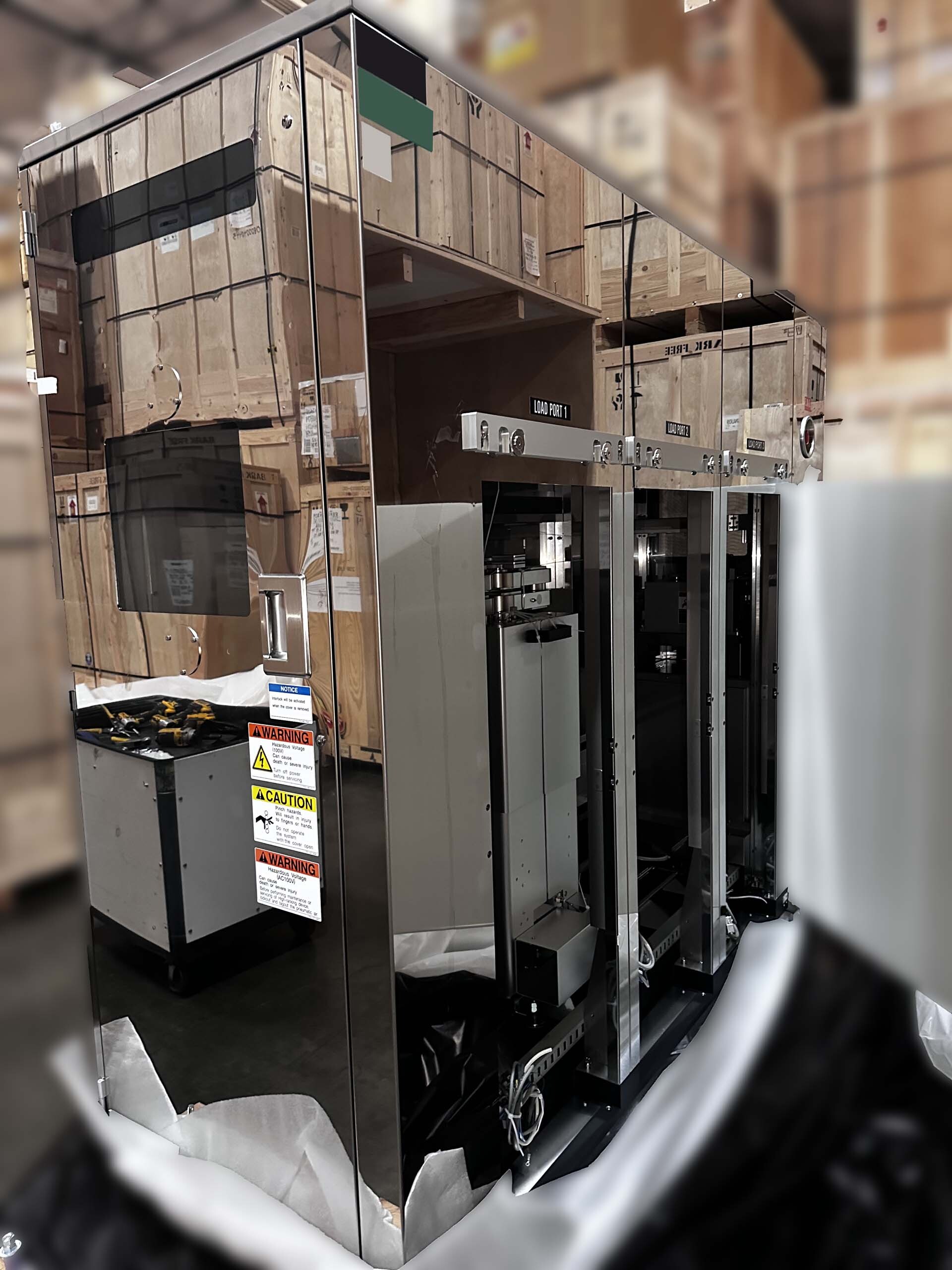
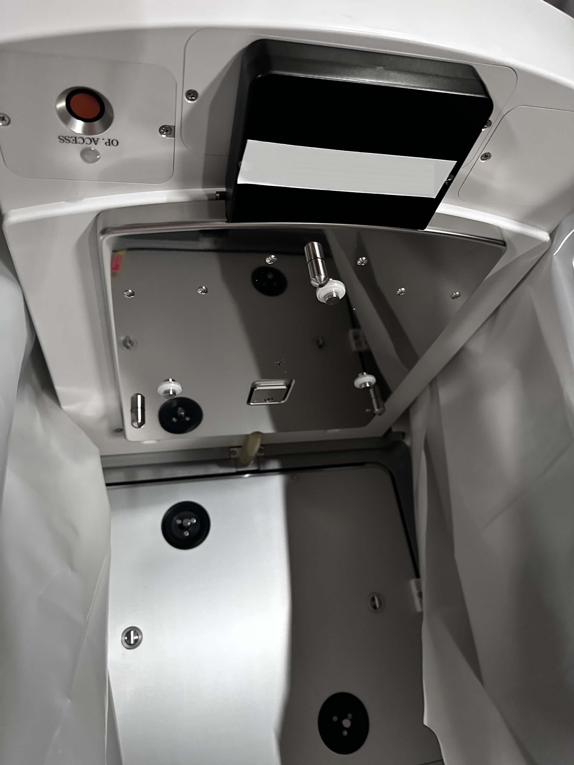
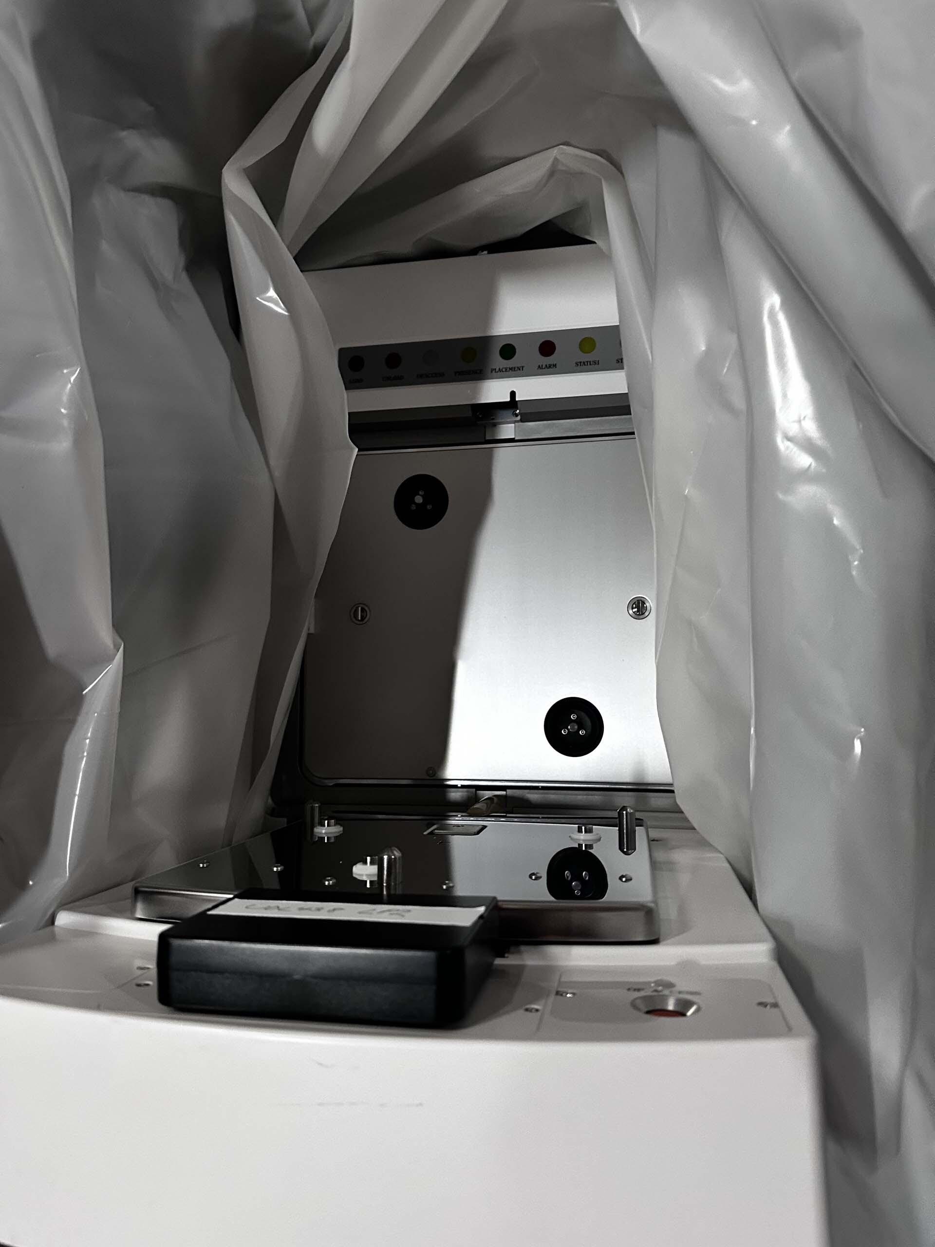
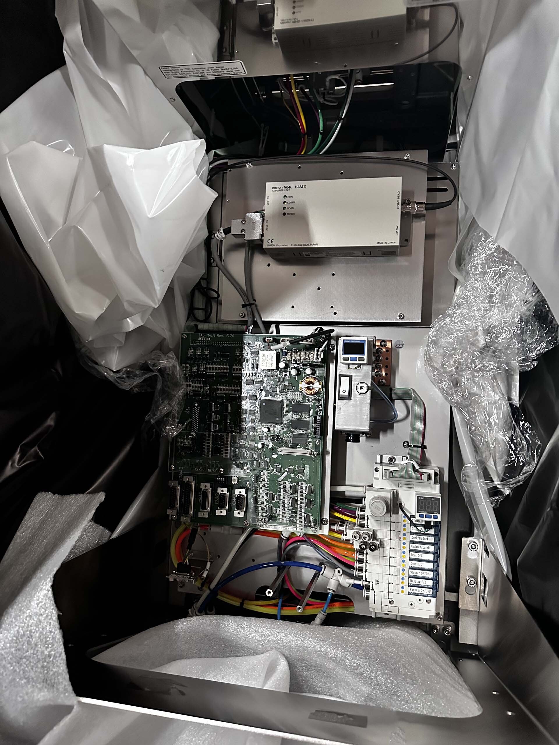
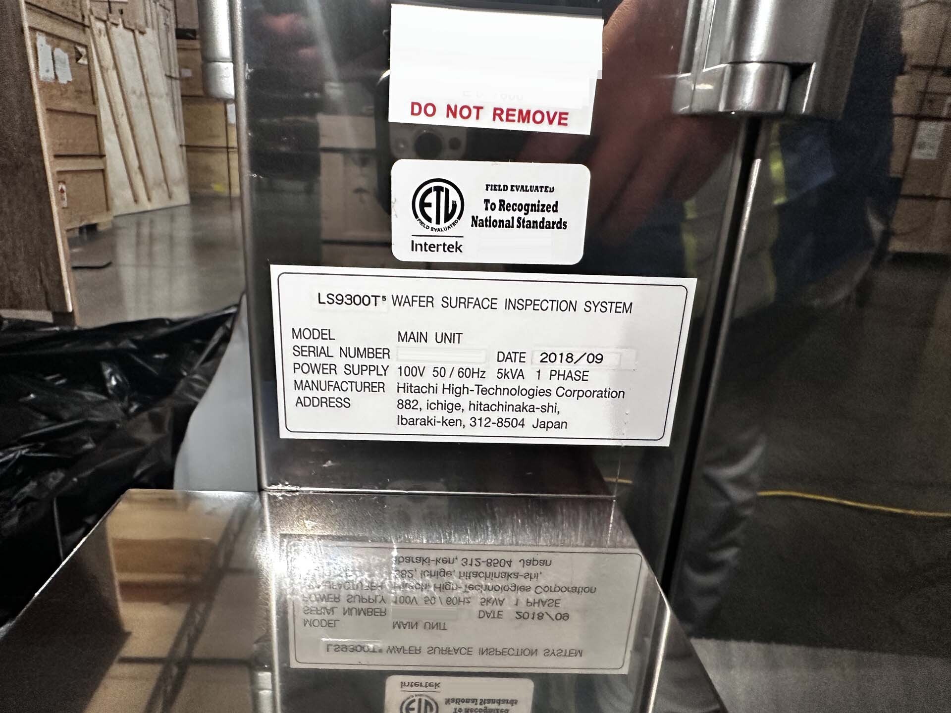
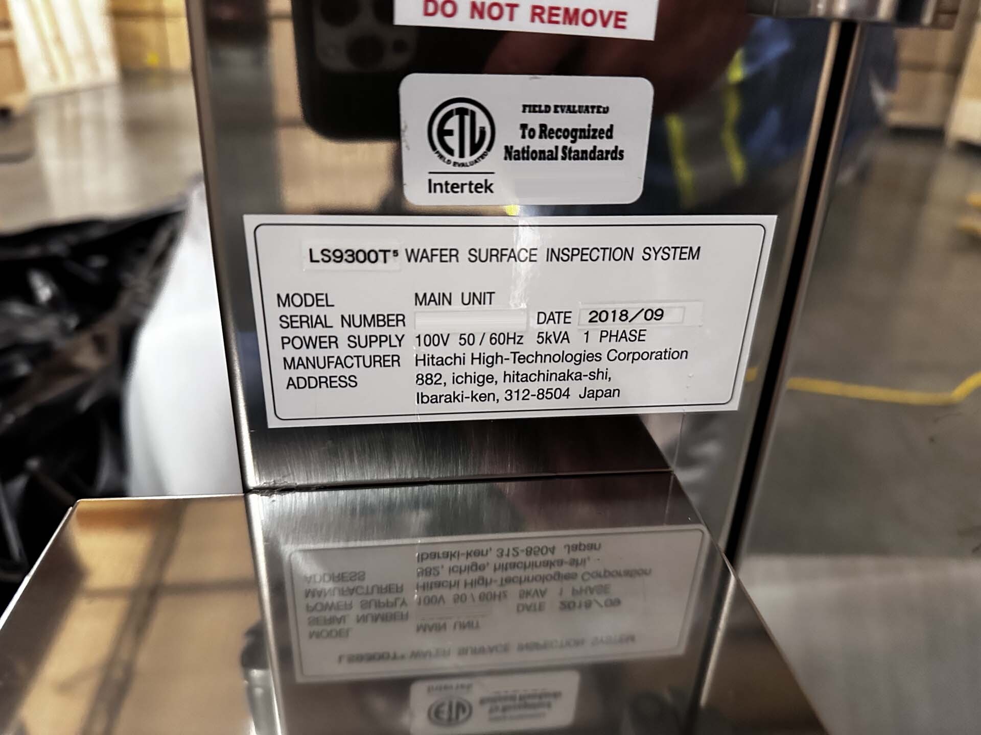
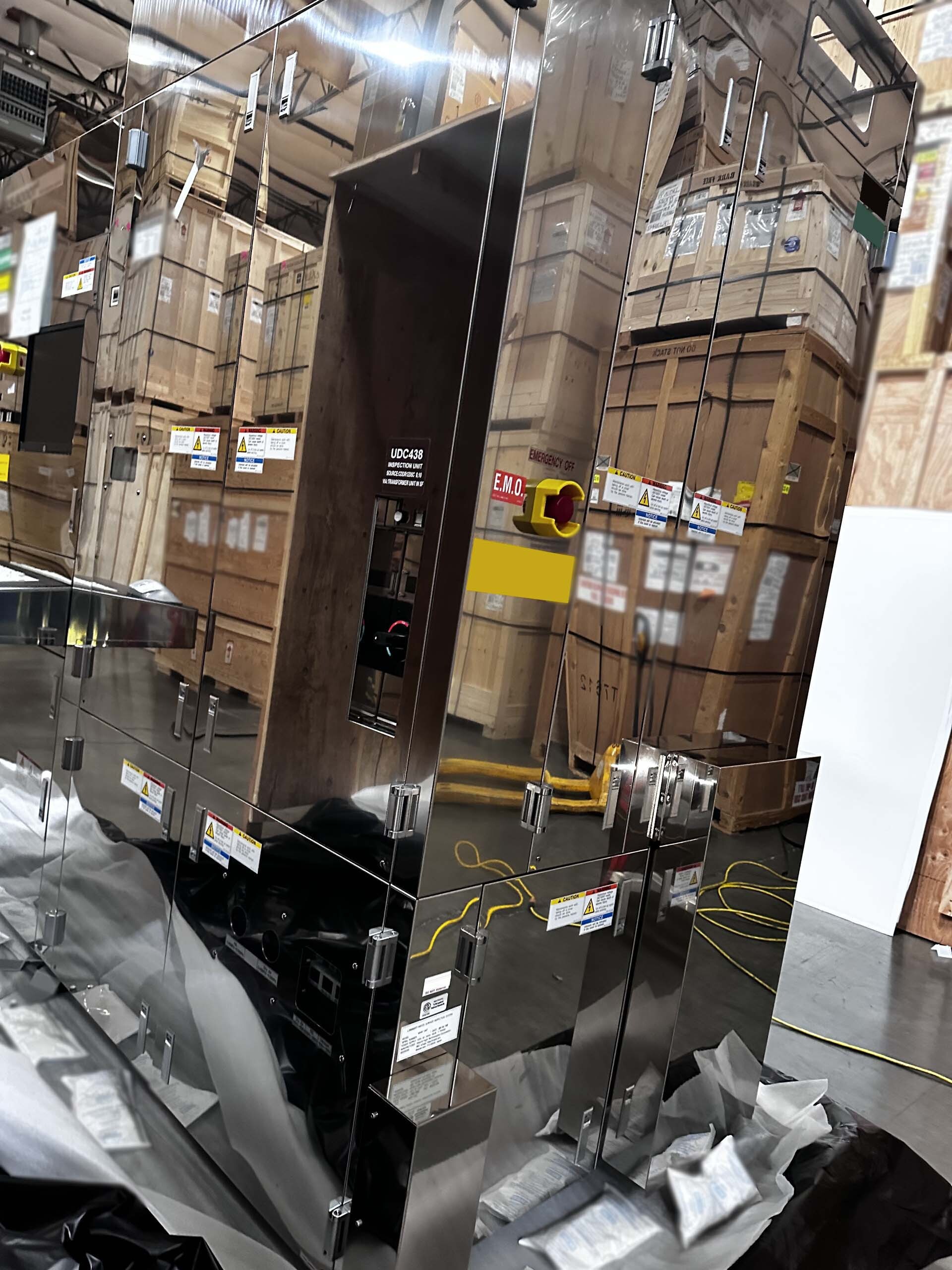
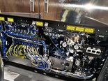
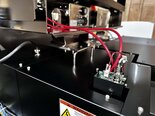
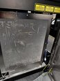
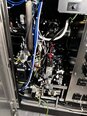
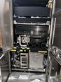
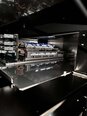
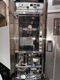
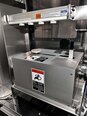
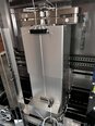
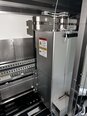
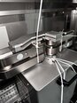
HITACHI LS 9300A+ is a state-of-the-art mask and wafer inspection equipment designed for the semiconductor industry. This system integrates advanced optical technologies and sophisticated algorithms to achieve high-resolution and high-speed inspection of masks and wafers used in the manufacturing of integrated circuits (ICs) and other semiconductor devices. LS 9300A+ is a crucial tool for ensuring the quality and reliability of semiconductor products by detecting defects and abnormalities that can affect the performance and functionality of the final devices. One of the key features of HITACHI LS 9300A+ is its advanced optical imaging unit, which utilizes a combination of bright-field and dark-field illumination techniques to capture detailed images of mask and wafer surfaces. The machine is equipped with a high-resolution microscope objective and an adjustable aperture to control the focus and depth of field, allowing for precise inspection of fine patterns and features on the samples. LS 9300A+ also incorporates advanced image processing algorithms to enhance image contrast and improve defect detection capabilities. HITACHI LS 9300A+ is equipped with multiple inspection modes, including pattern inspection, particle inspection, and overlay inspection, to address a wide range of defect types and sizes. The pattern inspection mode is used to detect defects such as missing patterns, line width variations, and pattern distortions that can result from mask or lithography process errors. LS 9300A+ utilizes advanced pattern recognition algorithms to compare captured images with reference patterns and identify deviations that may indicate defects. In particle inspection mode, HITACHI LS 9300A+ is capable of detecting and classifying particles and contaminants on mask and wafer surfaces that can negatively impact device performance and yield. The tool employs advanced image analysis techniques to differentiate between different types of particles, such as metallic or non-metallic contaminants, and determine their size, shape, and distribution across the samples. By detecting and categorizing particles, LS 9300A+ helps semiconductor manufacturers identify sources of contamination and improve process control measures to prevent future defects. Overlay inspection is another critical function of HITACHI LS 9300A+, enabling precise alignment and positioning of mask patterns on wafer substrates during the semiconductor fabrication process. The asset accurately measures overlay errors, such as misalignments and shifts between successive mask layers, to ensure the proper registration of patterns and optimize device performance. By detecting overlay defects early in the manufacturing process, LS 9300A+ helps semiconductor manufacturers reduce rework and improve production efficiency. Overall, HITACHI LS 9300A+ is a highly advanced mask and wafer inspection model that combines cutting-edge optical technologies with intelligent image processing algorithms to deliver superior defect detection and analysis capabilities for semiconductor manufacturing. With its versatile inspection modes, high-resolution imaging capabilities, and advanced defect classification features, LS 9300A+ enables semiconductor manufacturers to achieve the highest levels of quality and reliability in their products while enhancing production yields and reducing time-to-market.
There are no reviews yet