Used HITACHI WI-890 #293818810 for sale
URL successfully copied!
Tap to zoom
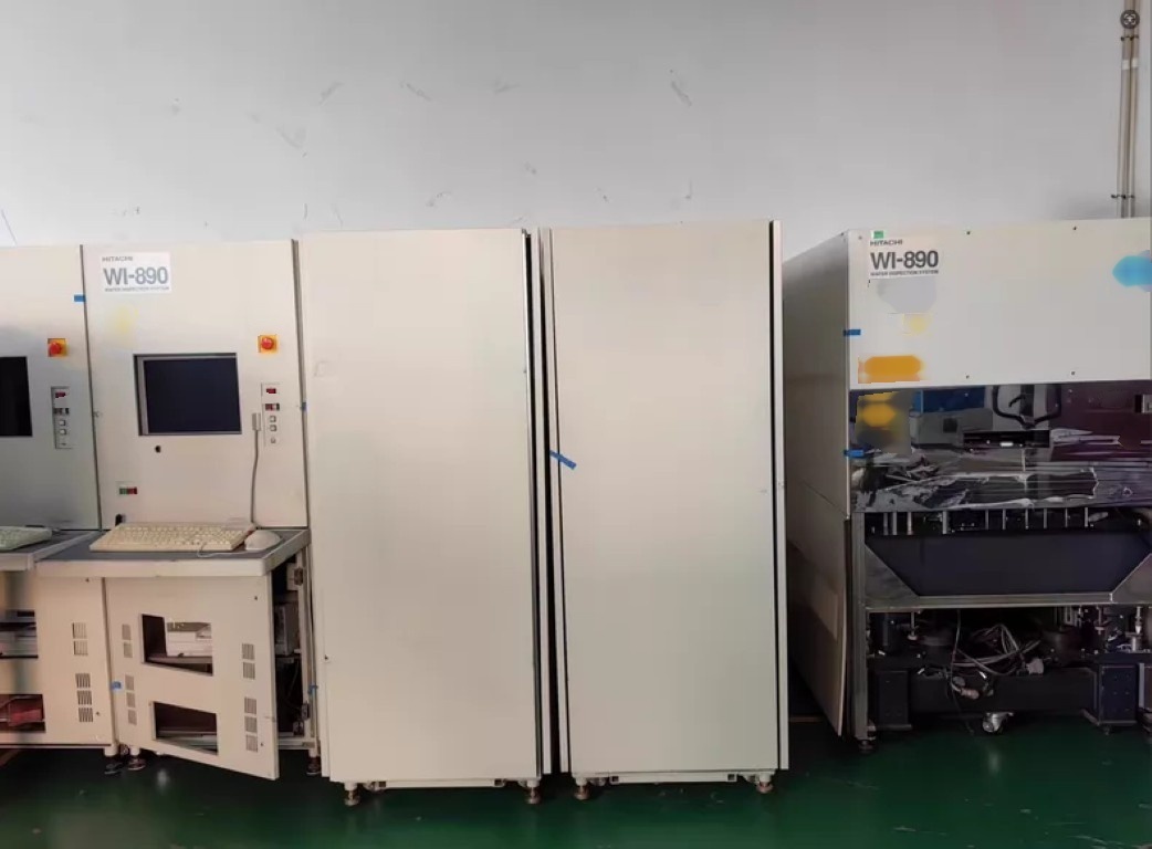

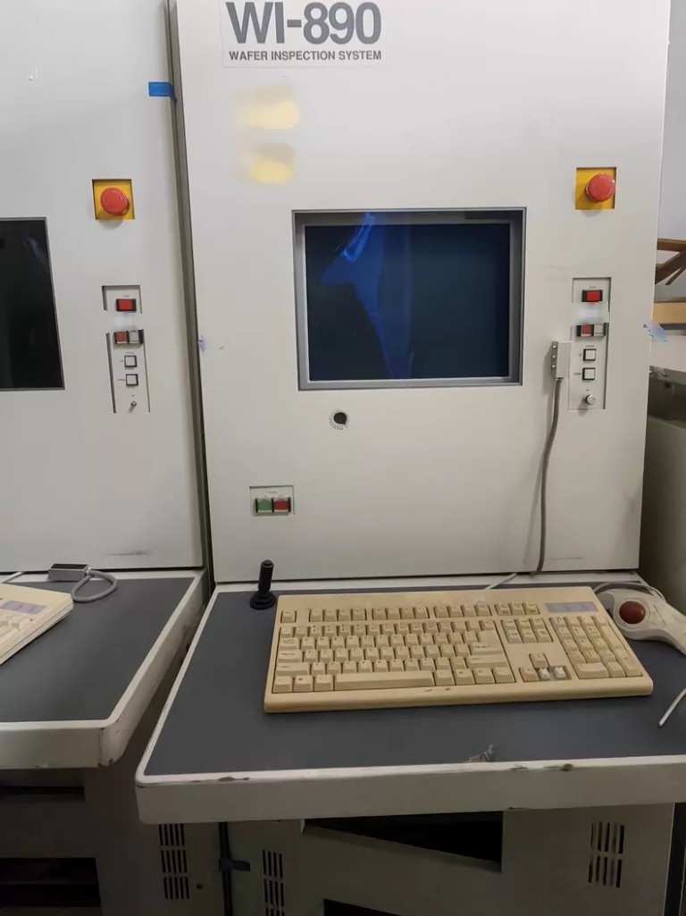
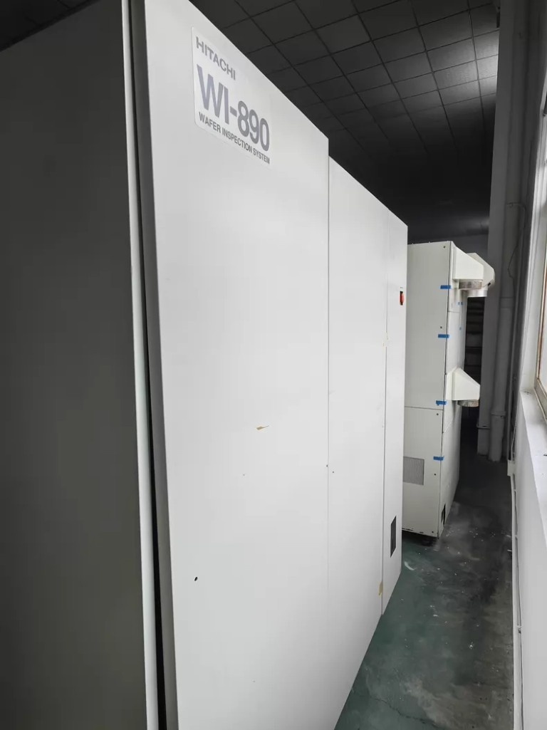
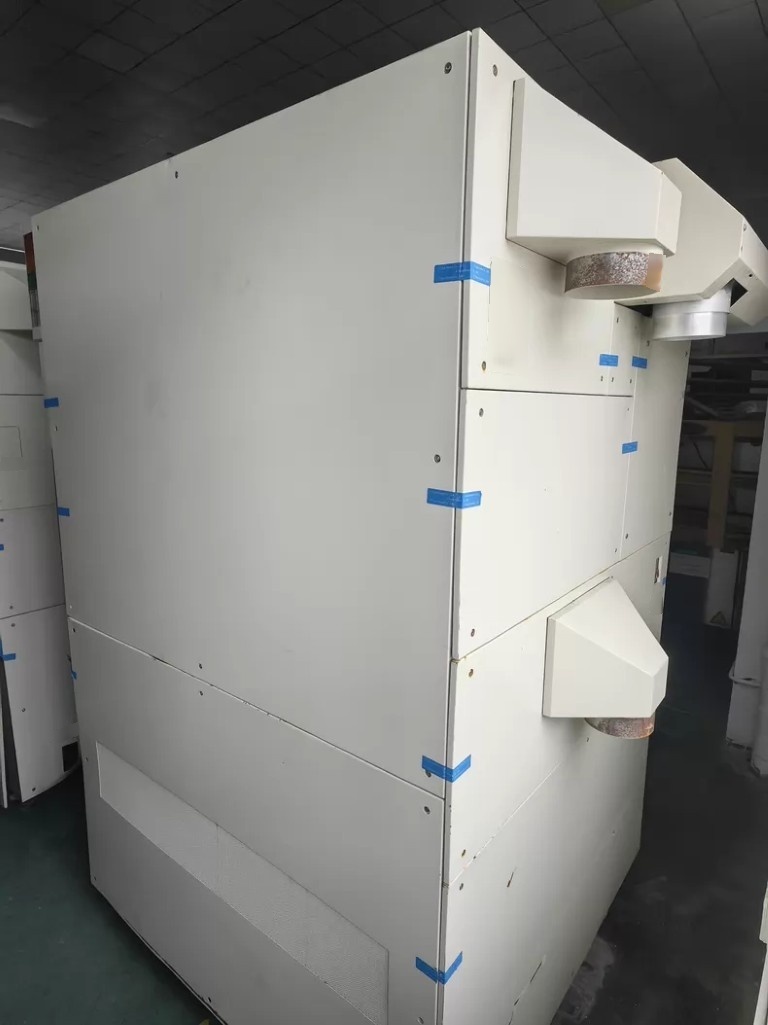
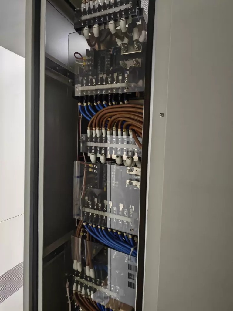
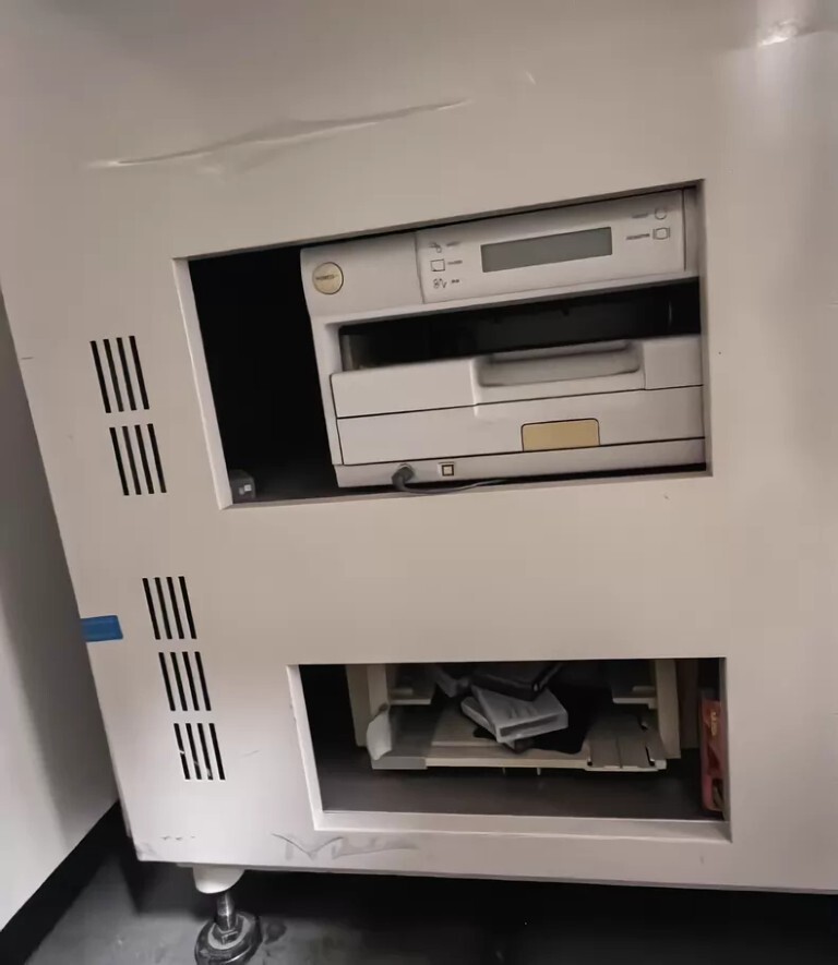
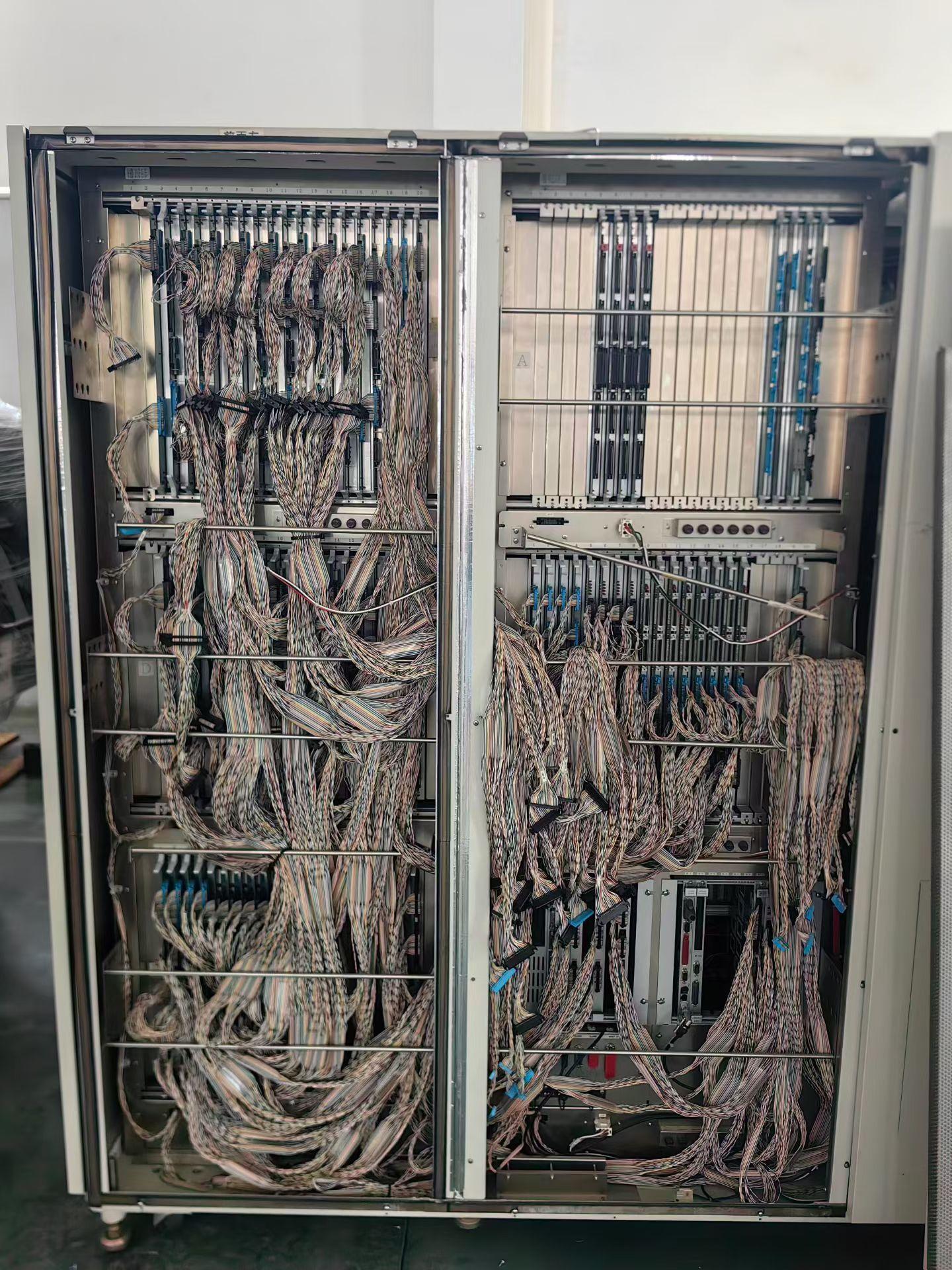
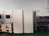
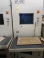
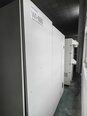
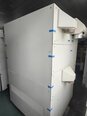
HITACHI WI-890 is an advanced mask and wafer inspection equipment designed to cater to the stringent demands of the semiconductor industry. This state-of-the-art system integrates cutting-edge technologies to enable accurate, reliable, and high-speed inspection of masks and wafers used in the fabrication of semiconductor devices. Equipped with sophisticated imaging capabilities and comprehensive inspection algorithms, HITACHI WI 890 is a versatile tool that provides precise defect detection and classification to ensure the quality and yield of semiconductor products. At the core of WI-890 is its advanced optical inspection technology, which leverages high-resolution imaging to capture detailed information about the surface of masks and wafers. The unit employs a combination of bright-field and dark-field illumination techniques to enhance contrast and improve the visibility of defects on the samples. Through a series of precision optics and filters, WI 890 is able to achieve superior image quality, allowing for the detection of even the tiniest defects that could impact device performance. One of the key features of HITACHI WI-890 is its capability to handle a wide range of sample sizes and types. The machine supports multiple sizes of masks and wafers, accommodating the diverse requirements of semiconductor manufacturers. Whether inspecting photomasks for lithography processes or wafer samples for semiconductor fabrication, HITACHI WI 890 offers flexibility and scalability to adapt to varying production needs. Moreover, WI-890 is equipped with advanced automation features to streamline the inspection process and improve productivity. The tool integrates robotic handling systems for loading and unloading samples, reducing manual intervention and minimizing the risk of contamination. Additionally, WI 890 is equipped with intelligent software algorithms that enable rapid scanning and analysis of samples, allowing for efficient defect identification and classification. In terms of performance, HITACHI WI-890 excels in providing accurate defect detection and characterization for masks and wafers. The asset is capable of detecting various types of defects, including particles, pattern deviations, and scratches, with high sensitivity and specificity. By utilizing advanced image processing algorithms and machine learning techniques, HITACHI WI 890 can differentiate between critical defects that may impact device functionality and non-critical anomalies that have minimal impact on quality. Furthermore, WI-890 offers comprehensive data analysis and reporting capabilities to support process optimization and quality control. The model generates detailed inspection reports that provide insights into defect trends, distribution maps, and statistical analyses, enabling manufacturers to identify root causes of issues and implement corrective actions swiftly. With its user-friendly interface and intuitive software tools, WI 890 empowers operators to make informed decisions and improve the overall efficiency of semiconductor manufacturing processes. In conclusion, HITACHI WI-890 is a leading-edge mask and wafer inspection equipment that delivers unparalleled performance, reliability, and flexibility for semiconductor manufacturing. With its advanced optical inspection technology, versatile sample handling capabilities, automated workflows, and sophisticated analysis tools, HITACHI WI 890 is a valuable asset for semiconductor manufacturers seeking to achieve superior product quality and yield in today's competitive market.
There are no reviews yet