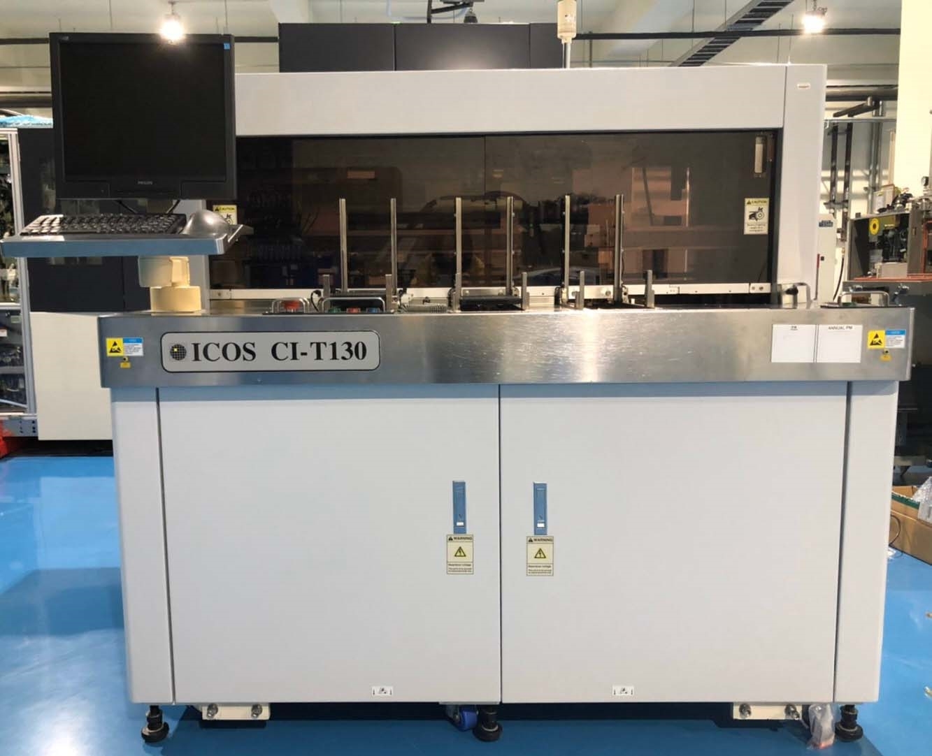
Used KLA / ICOS CI-T130 #9256514 for sale
It looks like this item has already been sold. Check similar products below or contact us and our experienced team will find it for you.
Tap to zoom


Sold
ID: 9256514
Vintage: 2008
Lead scanner
(10) Heads
Tray to tray
X1~X3
2D is RLM
3D is QLM (IVC-5000)
Top mark: IVC-4000
Top plate: 86 x 86
Operating system: Windows 10.2
Manual included
Power supply: 220 AC
2008 vintage.
KLA / ICOS CI-T130 Mask & Wafer Inspection Equipment is a leading-edge automated inspection platform designed to inspect a range of semiconductor parts, including masks and wafers. The system enables production engineers to quickly and accurately conduct defect detection, defect characterization, and other important tasks. A fast processing unit with advanced algorithms and high-level automation allows the highly precise and efficient scanning of devices and provides extremely accurate and reliable defect analysis results. KLA CI-T130 uses a 3D image sensor and a 2D sensor to scan objects for defects. The 3D image sensor can detect all types of defects, including scratches, smudges, contamination and other types of physical damage that cannot be detected by regular optical techniques. It features high resolution imaging of up to 30 μm and a 0.1 μm defect size resolution. The 2D sensor scans up to 50 μm into the substrate of the mask/wafer and measures chromatic shift from patterns to determine pass or fail. ICOS CI-T130 can detect and identify defects on all types of masks and wafers, including DRAMs, Flash Memory, SOI (Silicon on Insulator) wafers, 3D-NAND and other complex semiconductor devices. The machine also supports a range of inspection modes, such as Macro Inspection, Micro Inspection, and Low Magnification Inspection. Its high bulk scanning speed enables fast and reliable inspection for a large number of objects in a short time period. The tool is capable of defect-based classifying, data correlated cross-function inspecting and pattern matching. It enables users to effectively search and compare scanned images for a variety of defect characteristics from multiple light sources and wavelengths. This helps users to accurately identify any potential problems with masks/wafers. The asset also has advanced defect tracking capabilities which enables users to quickly identify and compare patterns of recurring defects. Overall, CI-T130 is an efficient and reliable mask and wafer inspection model that helps semiconductor engineers to rapidly detect and identify mask/wafer defects. Its advanced features and capabilities help to provide highly accurate and reliable defect analysis results quickly.
There are no reviews yet