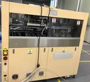
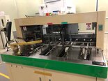
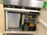
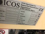
Used KLA / ICOS CI-T1X0 #9351871 for sale
URL successfully copied!
Tap to zoom
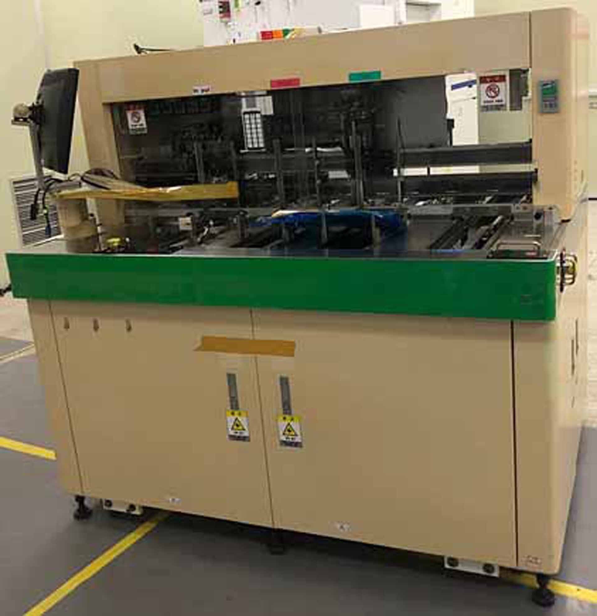

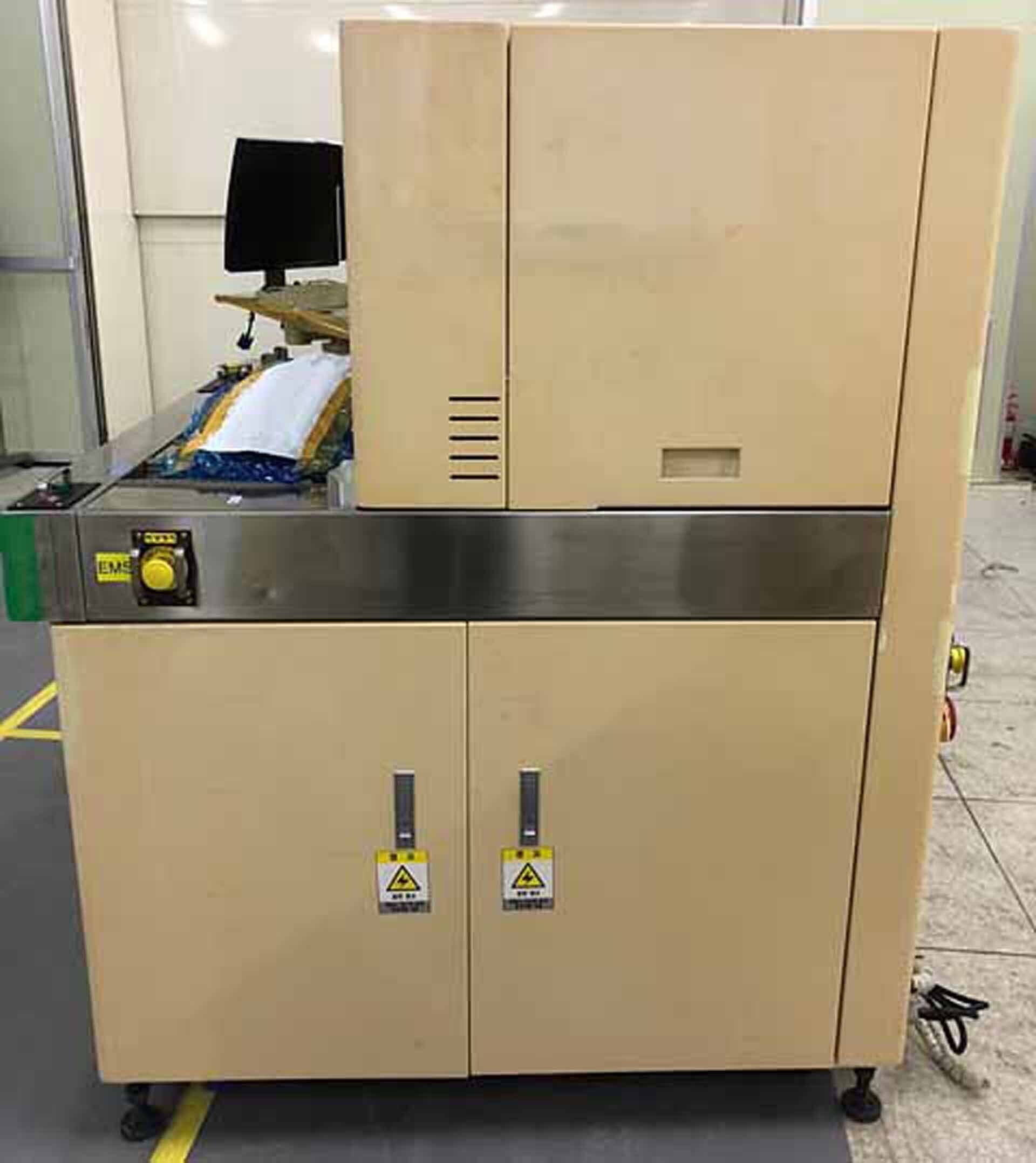

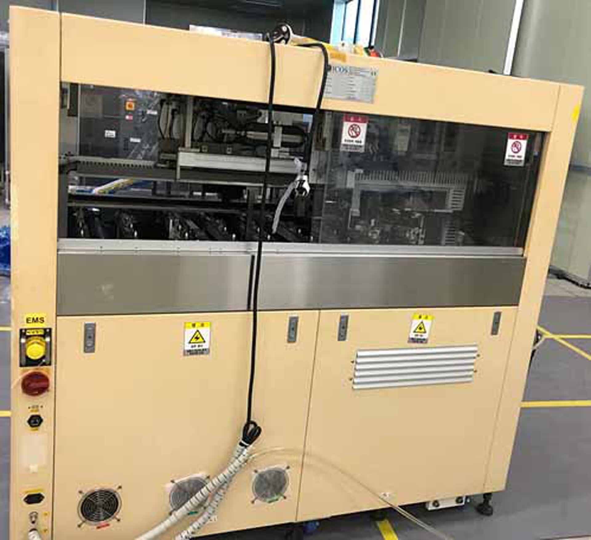

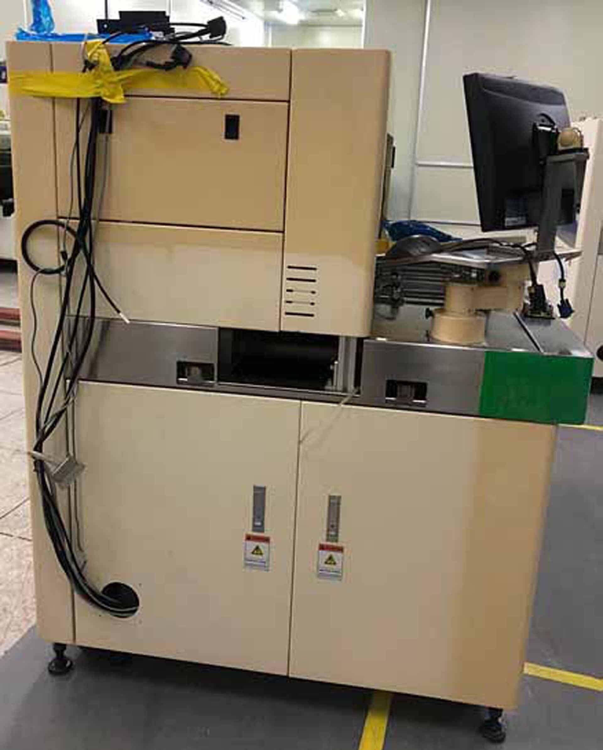


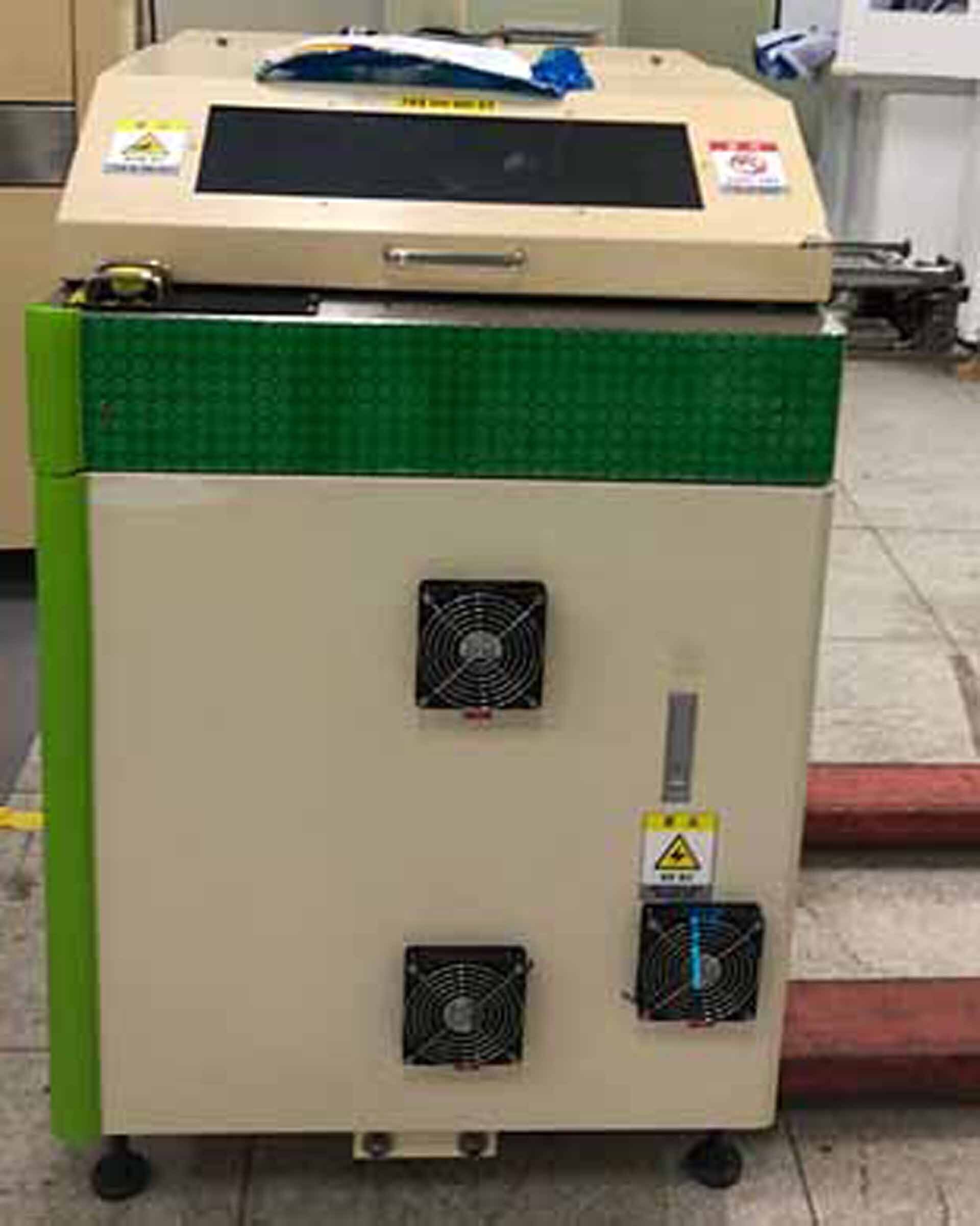

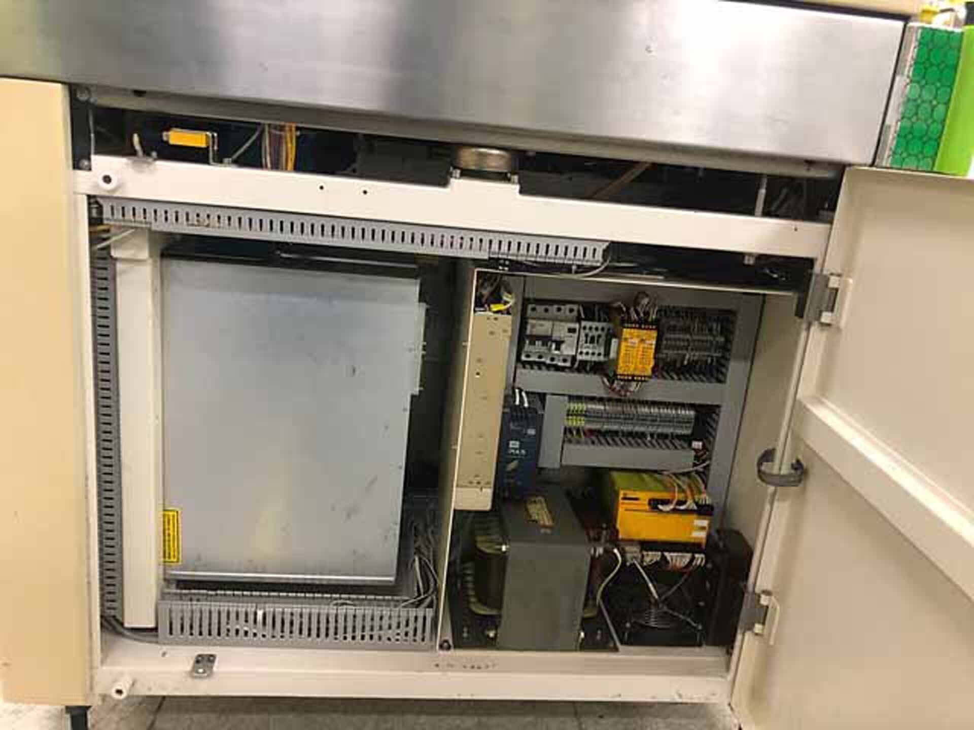

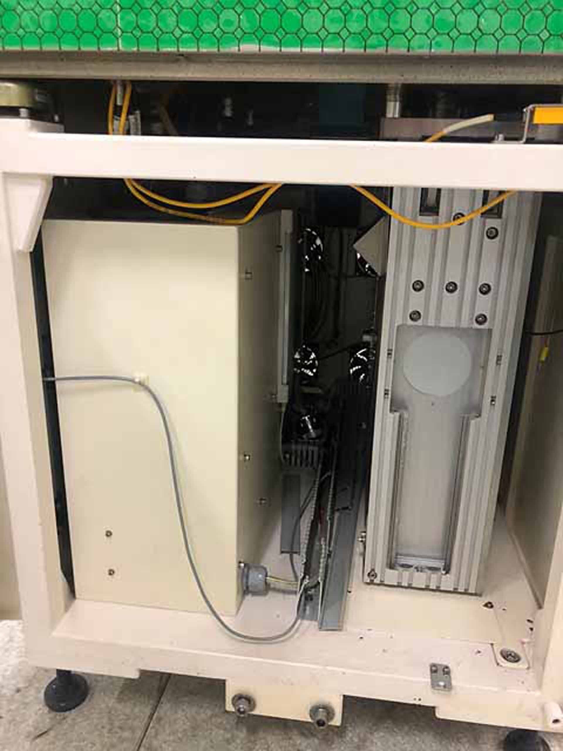

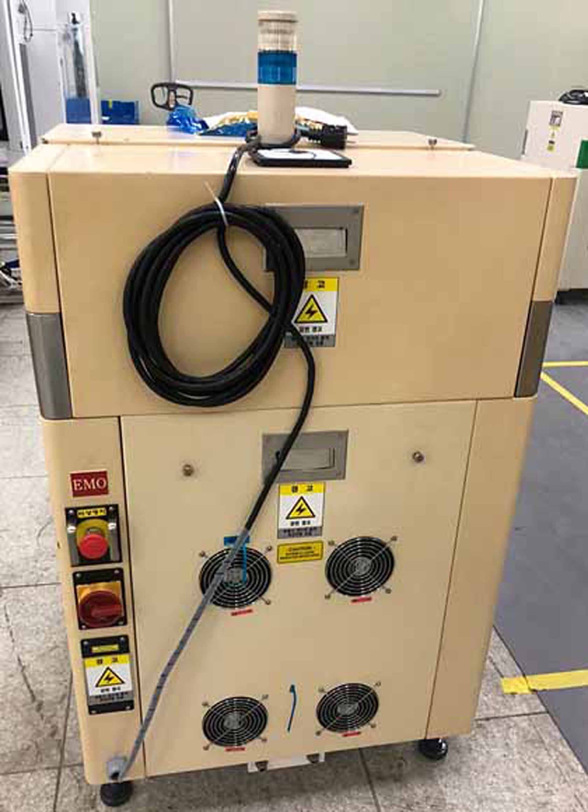

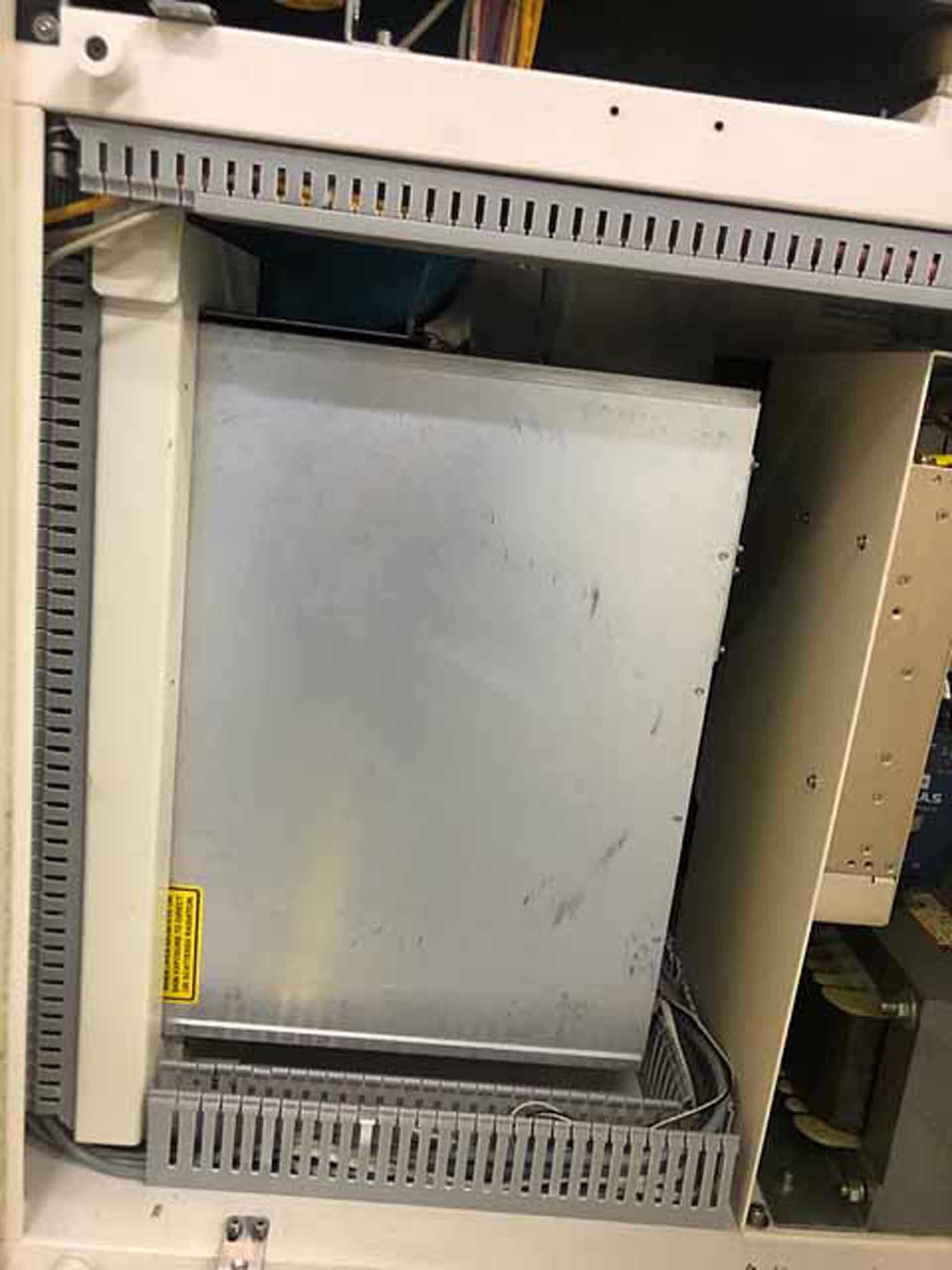

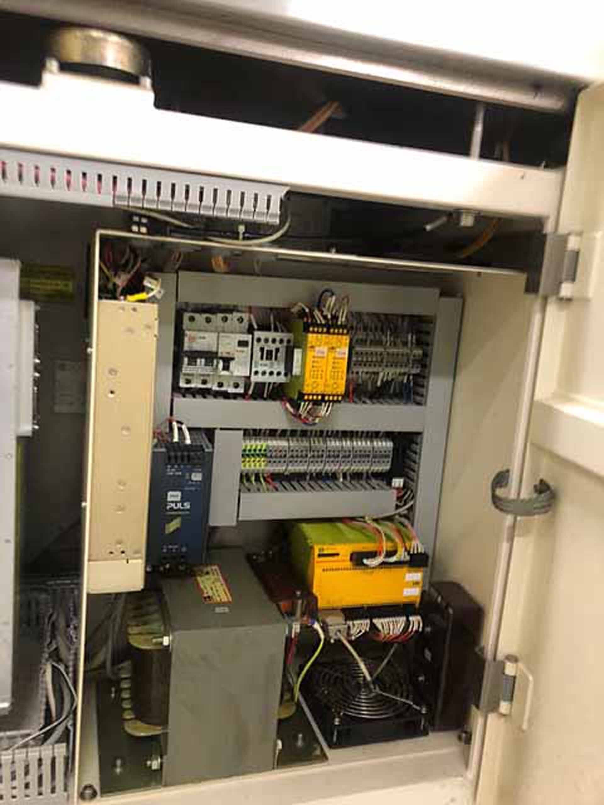

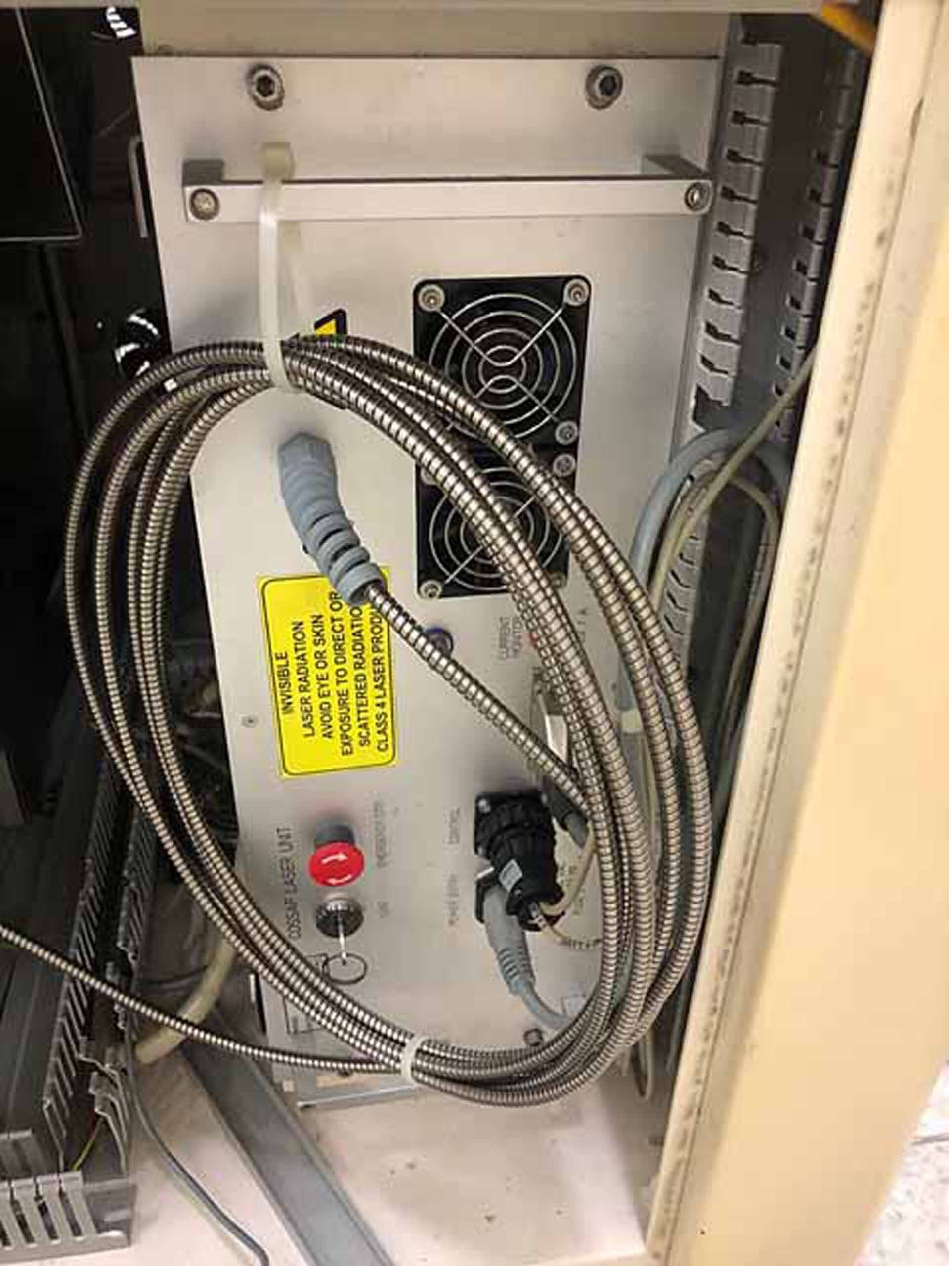

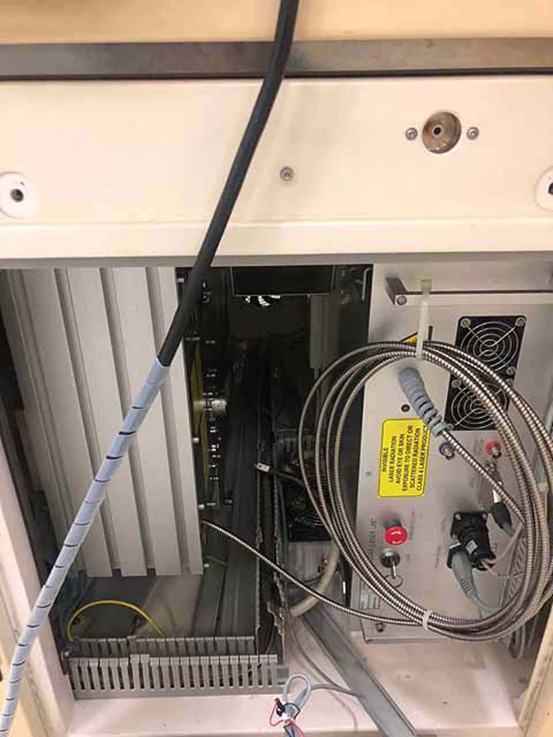

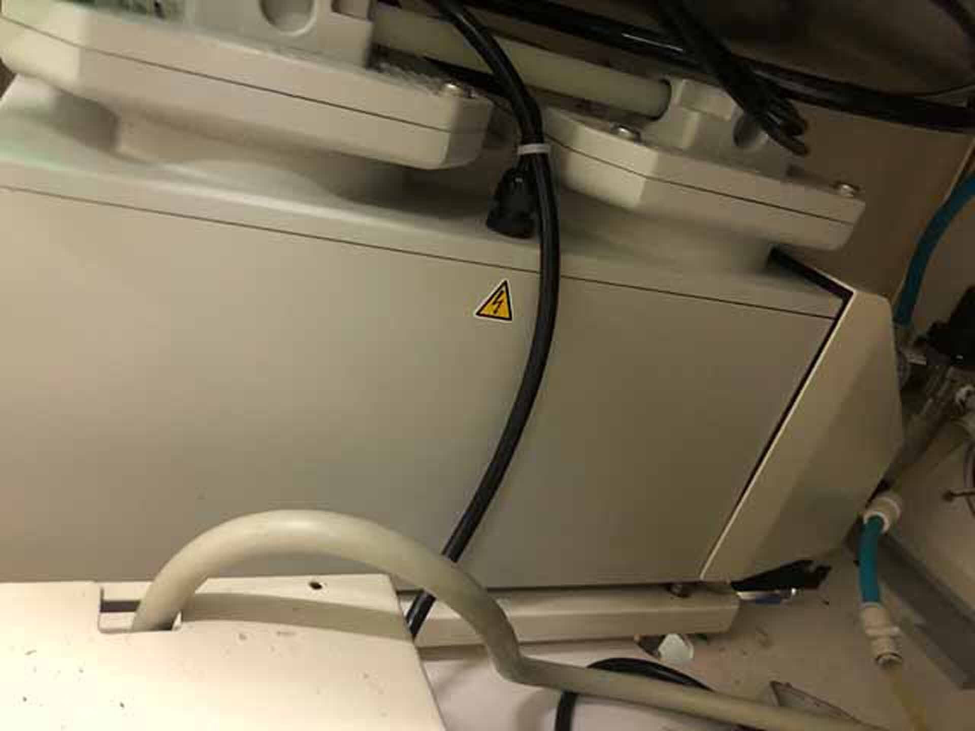


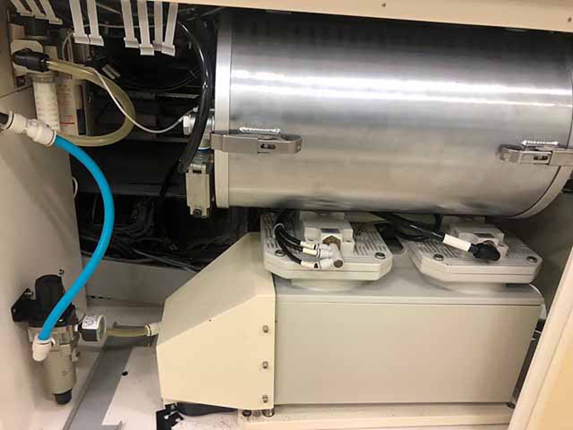


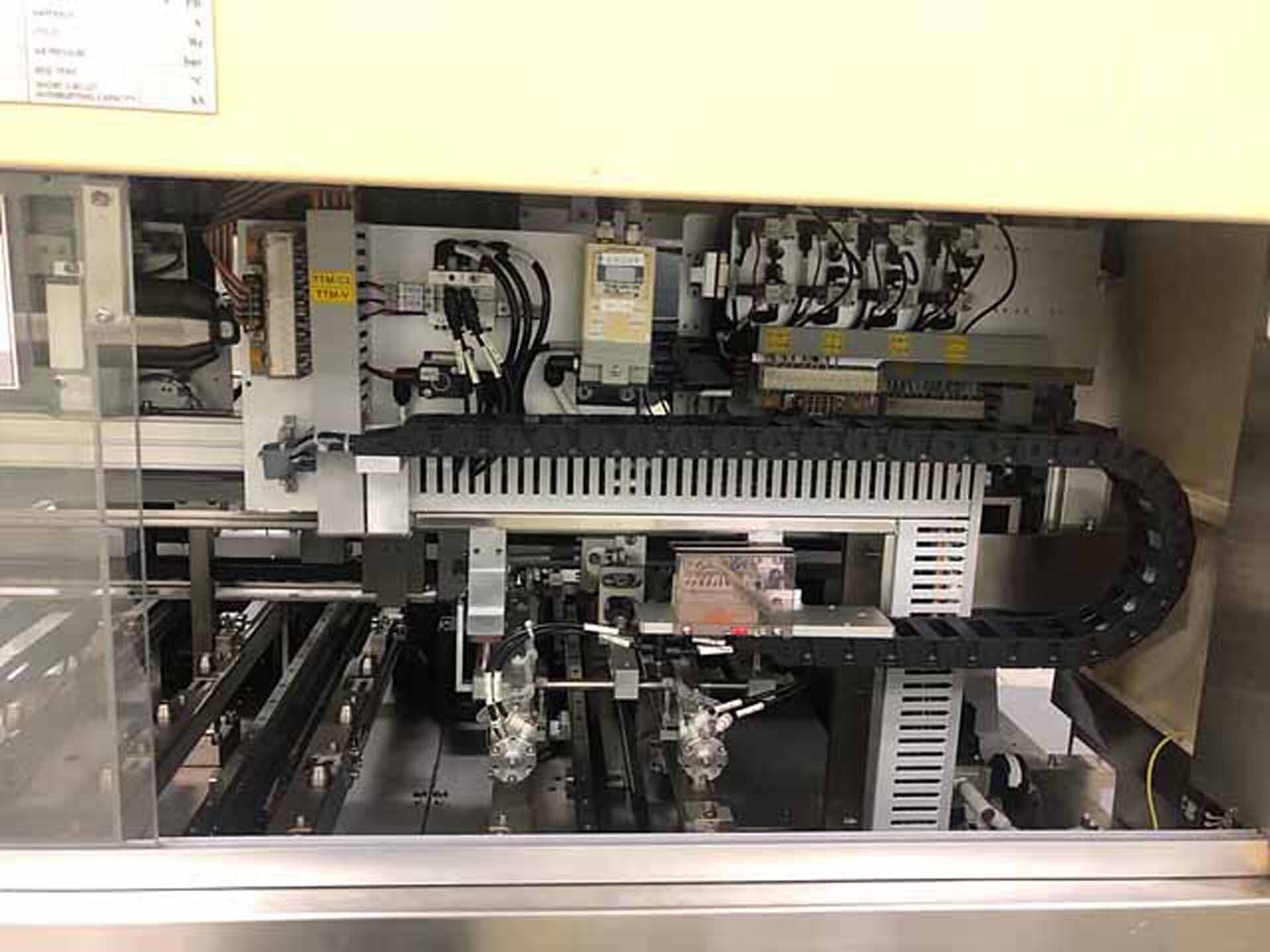


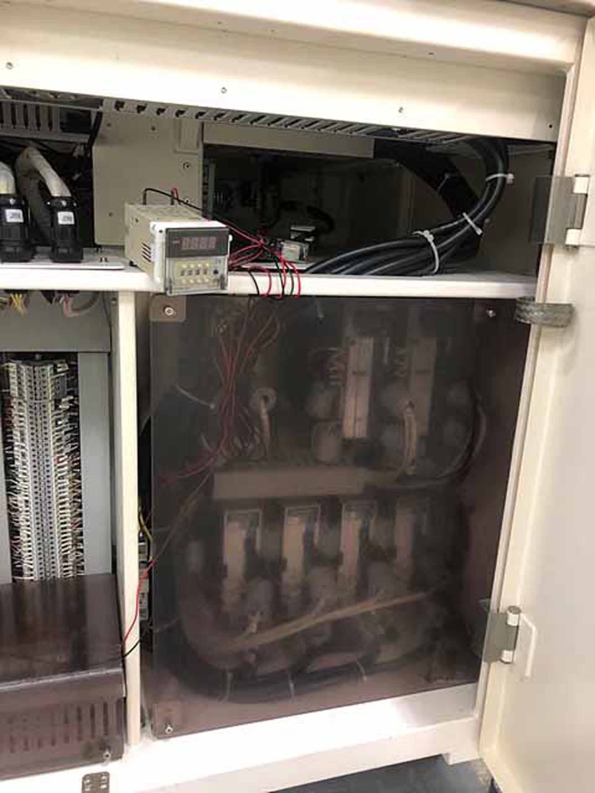

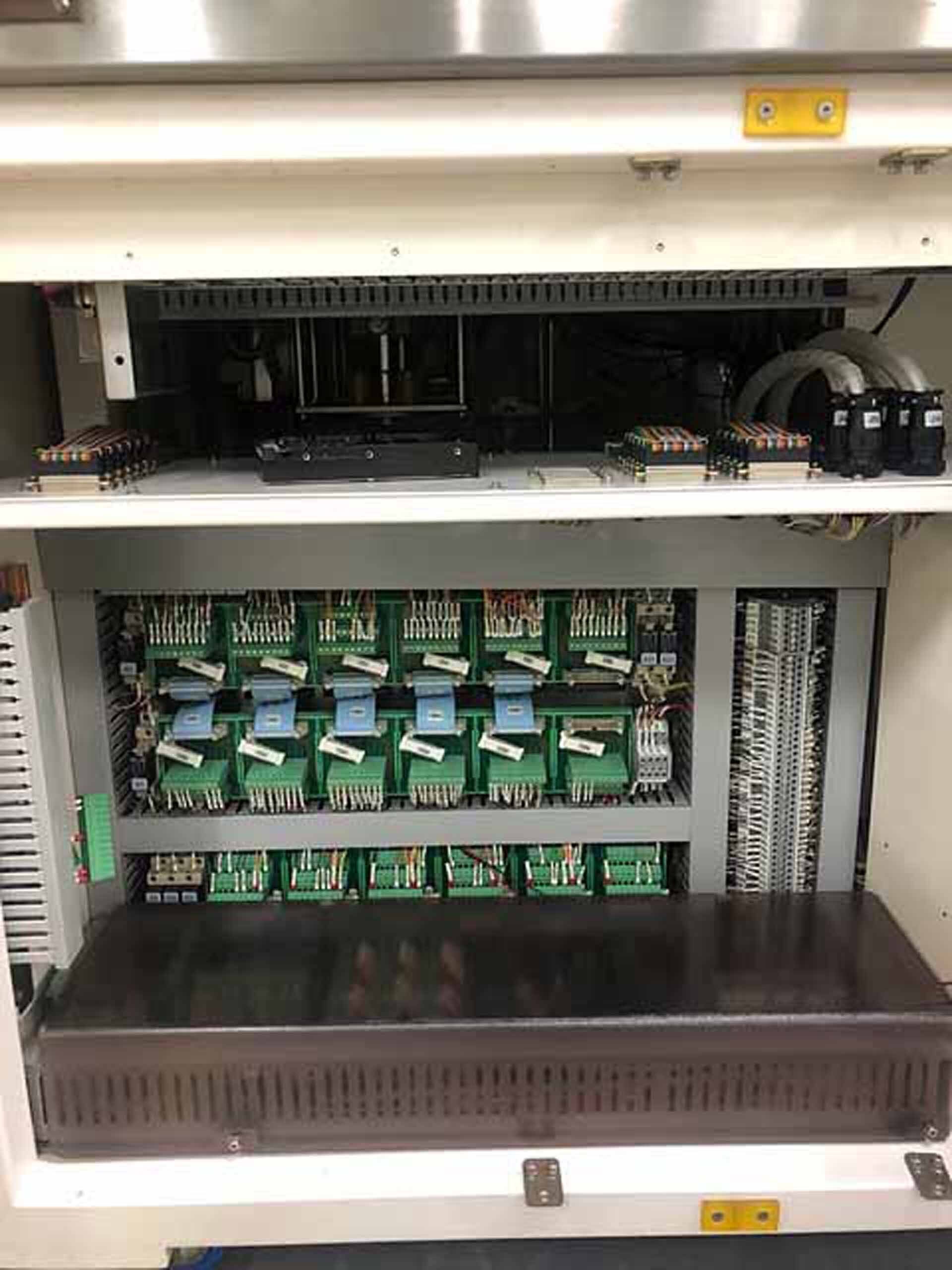


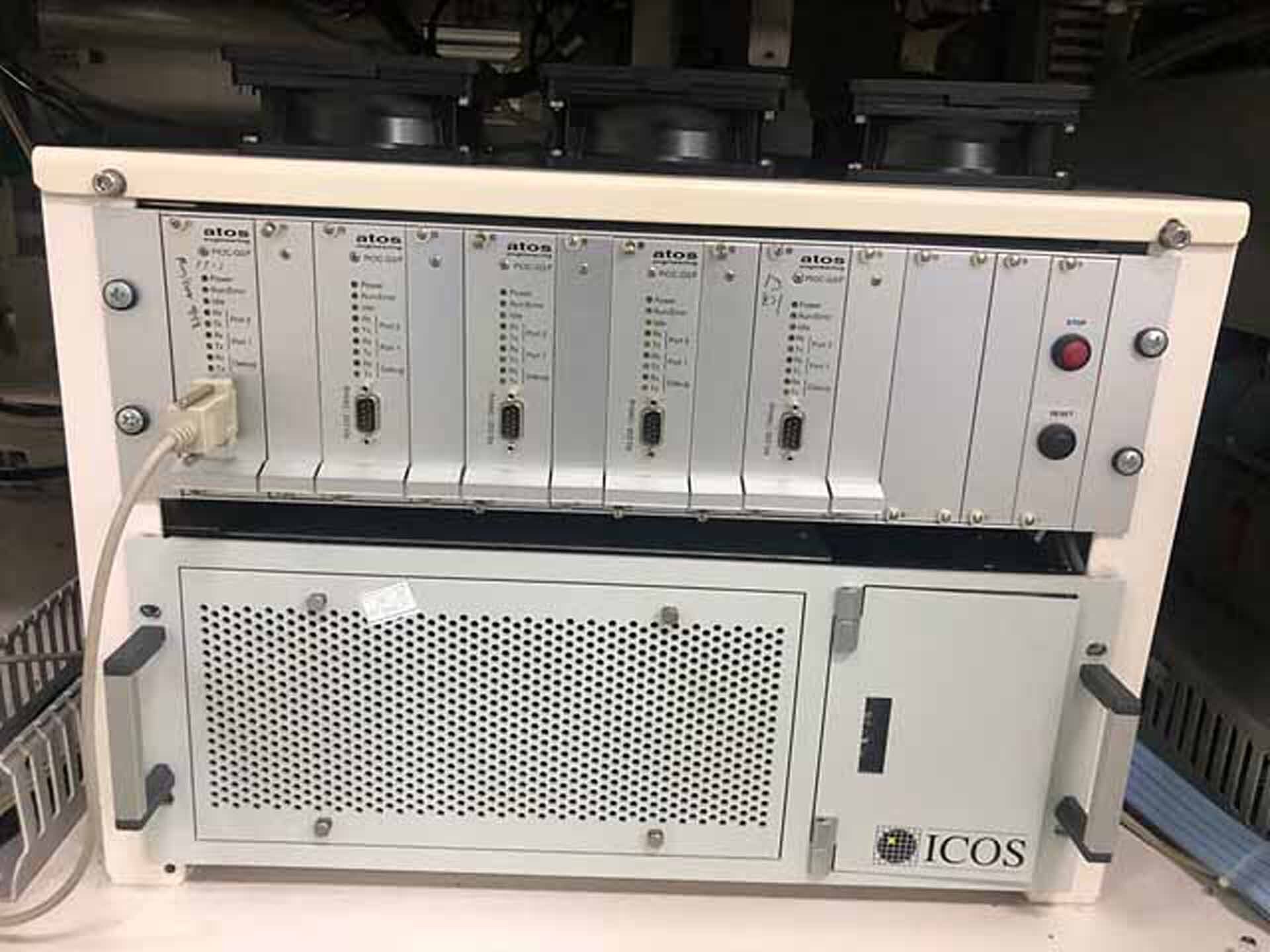

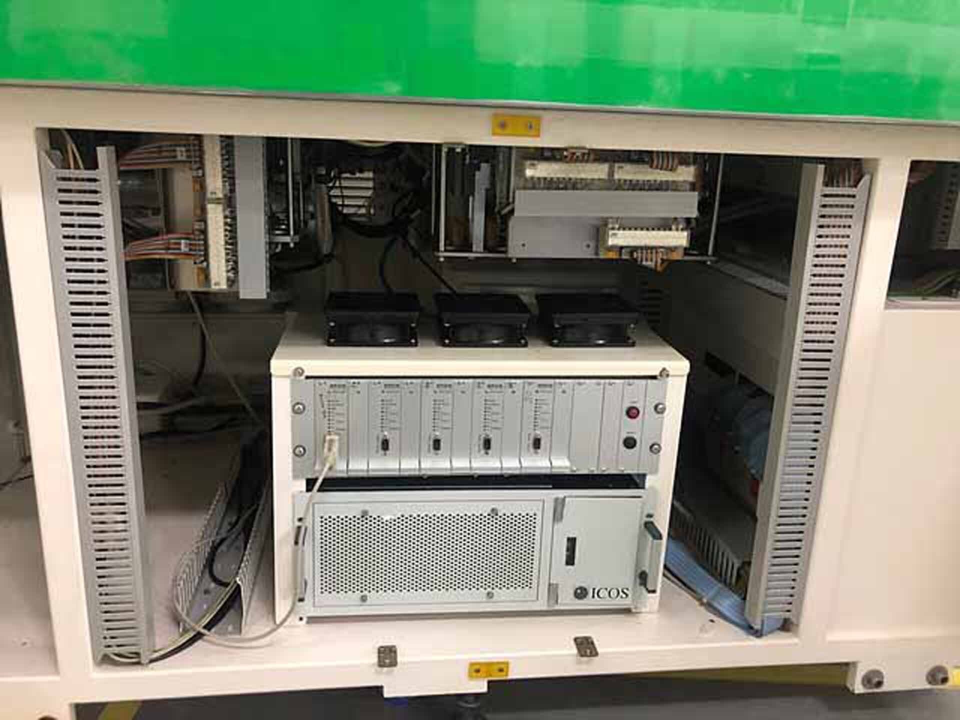

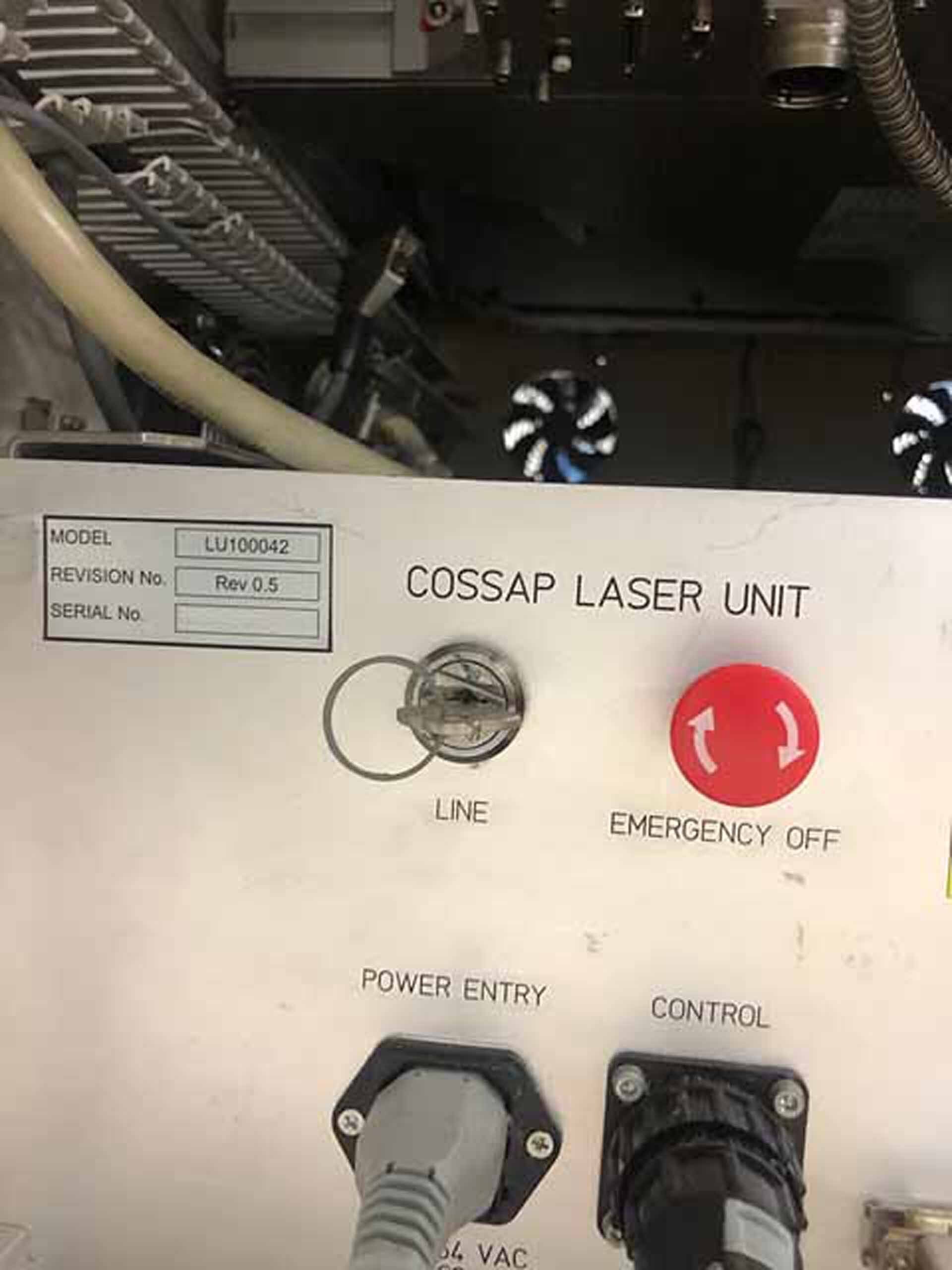

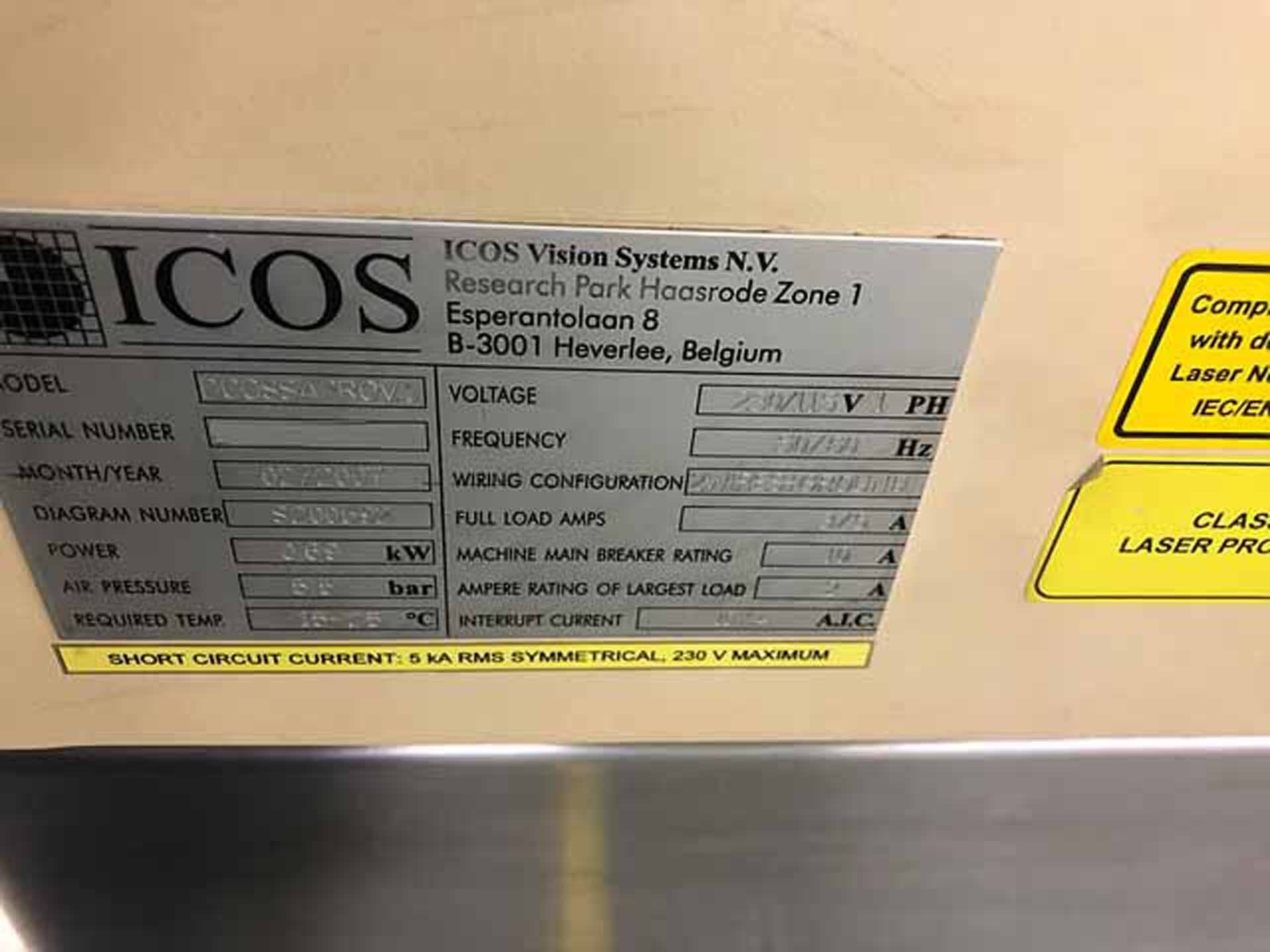

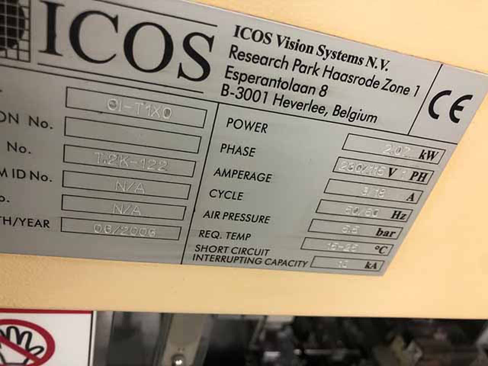

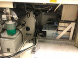
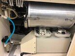
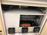
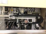
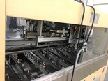
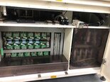
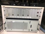
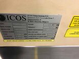
KLA / ICOS CI-T1X0 is a mask & wafer inspection equipment used in the fabrication of integrated circuits. It is specifically used for inspecting patterns formed on the masks and wafers used in the IC manufacturing process. The system is comprised of several components included automated pattern recognition, surface inspections, profile measurements, overlay measurement, cooling showers, and light sources. The automated pattern recognition in KLA CI-T1X0 unit is used to determine the presence of any defects in the mask and wafers. It inspects a wide range of features, such as contacts, vias, resistors, and capacitors. It also looks for defectives and contaminants on the surfaces and edges of the wafers. The surface inspections are used to identify any flaws or foreign material present on the mask and wafers' surfaces. These surfaces can be inspected across a range of magnifications using bright-field, dark-field, and contrast inverting techniques. The profile measurements can be used to measure the thickness and thickness variations of the masks and wafers. These measurements are also used to determine the relationships between the various material layers and substrates, as well as any voids or other discontinuities. The overlay measurements are used to measure the alignment of the different materials and masks used in the IC manufacturing process. It also helps to ensure that the different layers are properly bonded together. The cooling showers are used to keep the mask and wafers cool during the inspection process. This helps to reduce the risk of thermal damage occurring to the materials. Finally, the light sources in ICOS CI T1X0 are designed to illuminate the materials at different wavelengths. This allows for a detailed analysis of the masks and wafers, revealing any flaws or impurities present. Overall, KLA / ICOS CI T1X0 mask & wafer inspection machine is an invaluable tool used for ensuring the quality of integrated circuits produced using the IC manufacturing process. Thanks to its automated pattern recognition, surface inspections, profile measurements, overlay measurements, cooling showers and light sources, the tool can accurately detect any defects present in the ICs.
There are no reviews yet


