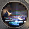
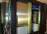
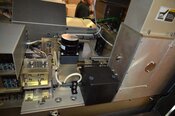
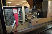
Used KLA / TENCOR 2122 #293644919 for sale
URL successfully copied!
Tap to zoom


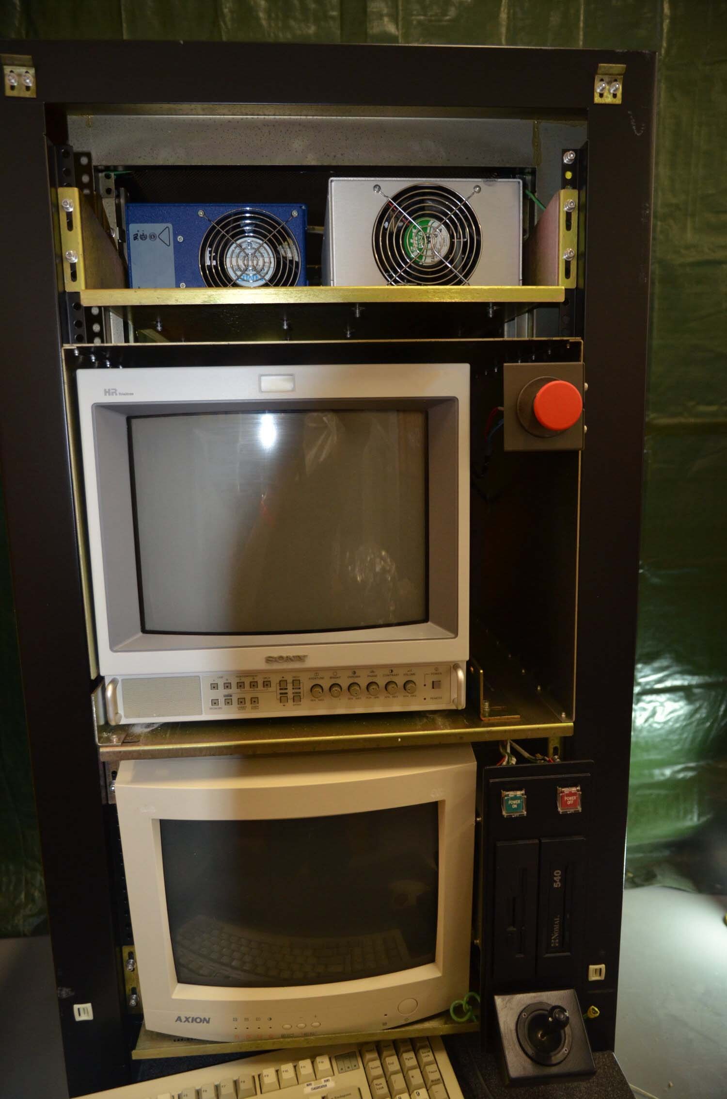

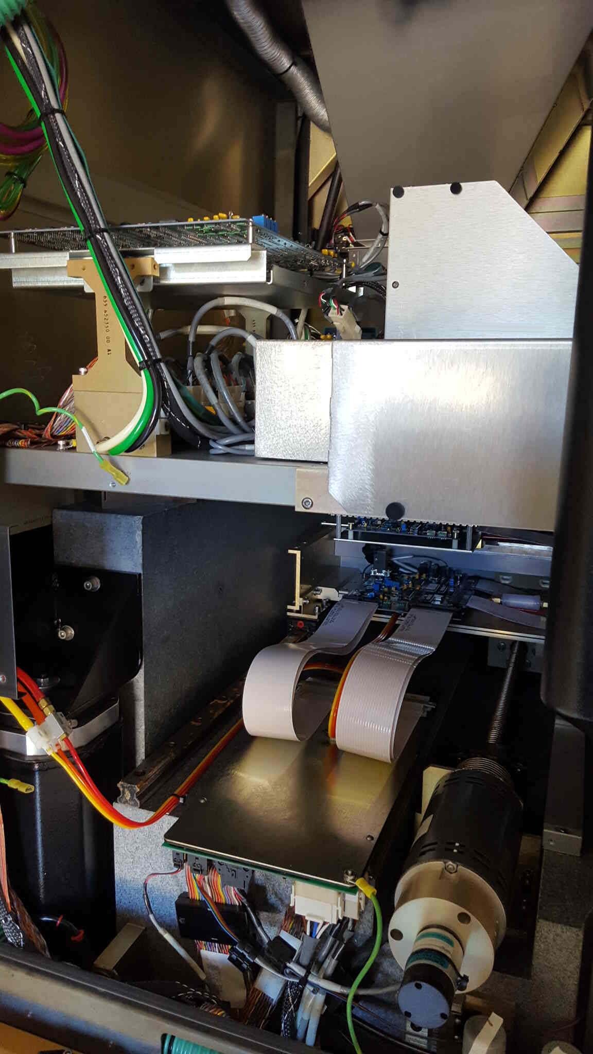

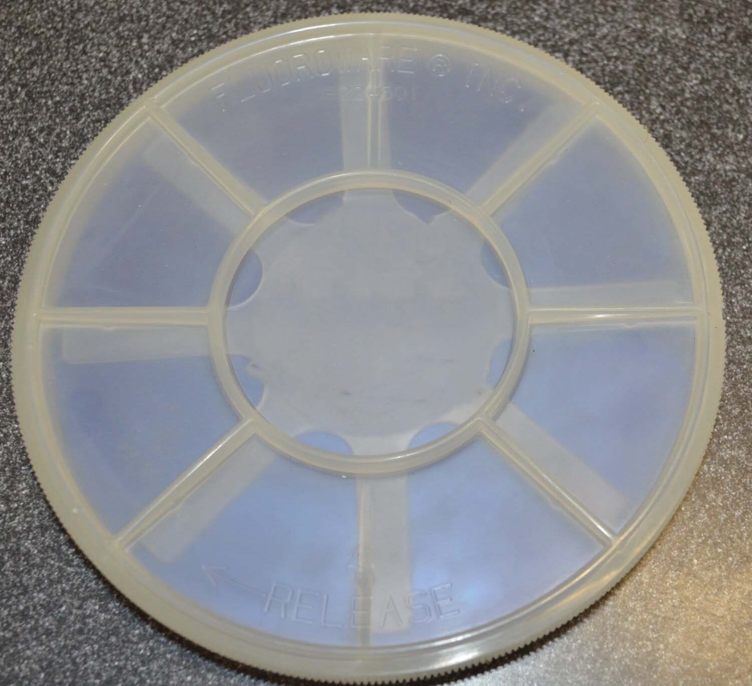


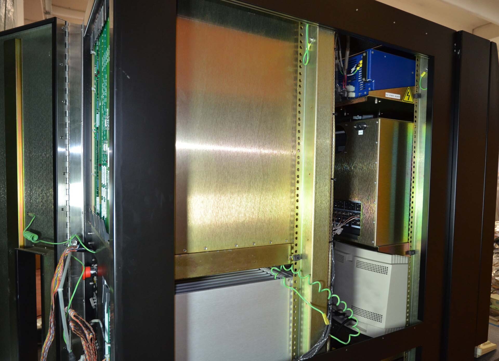

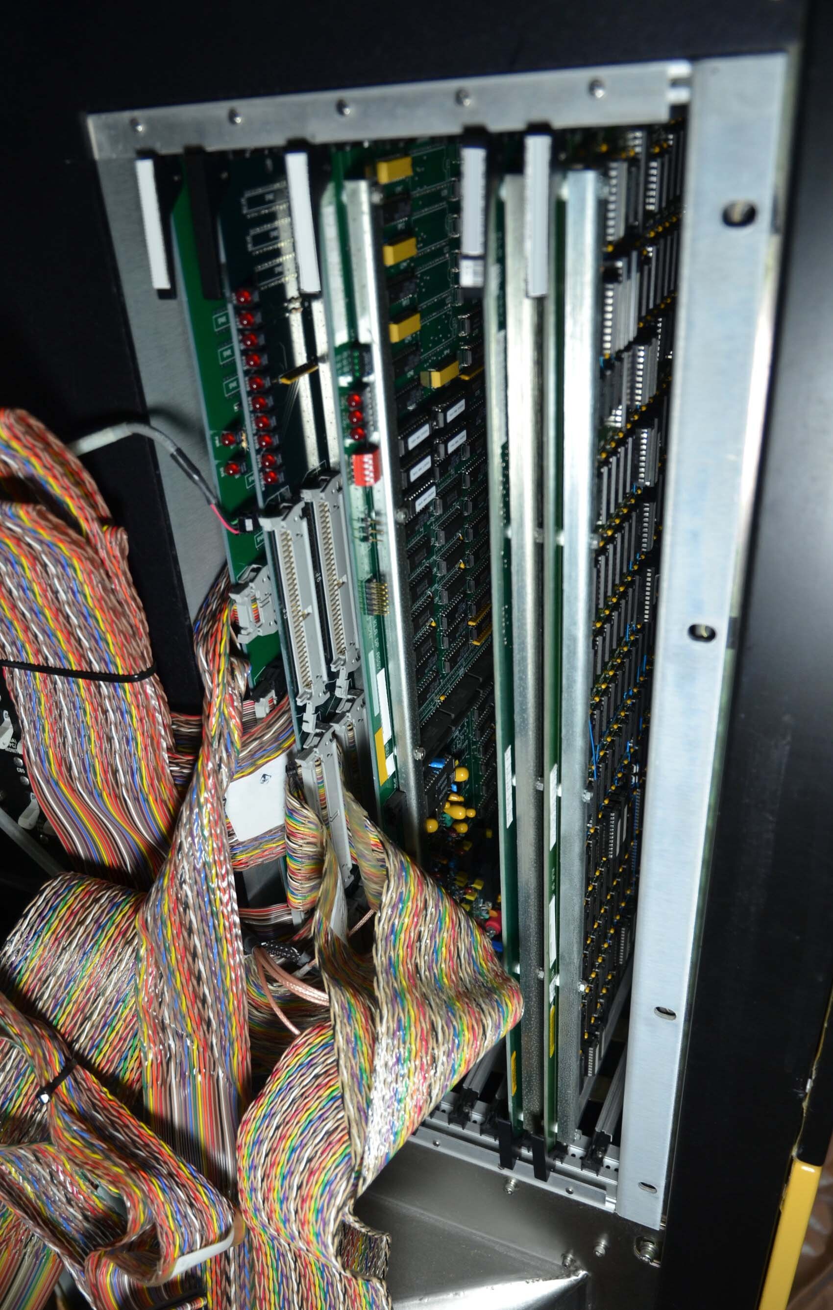

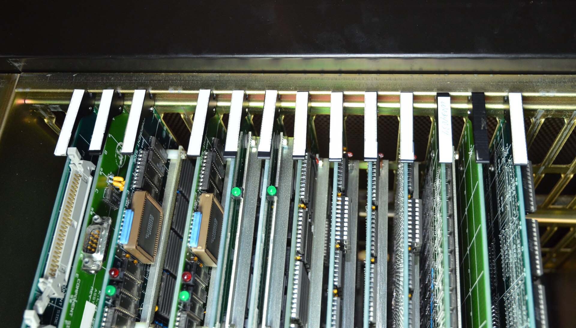

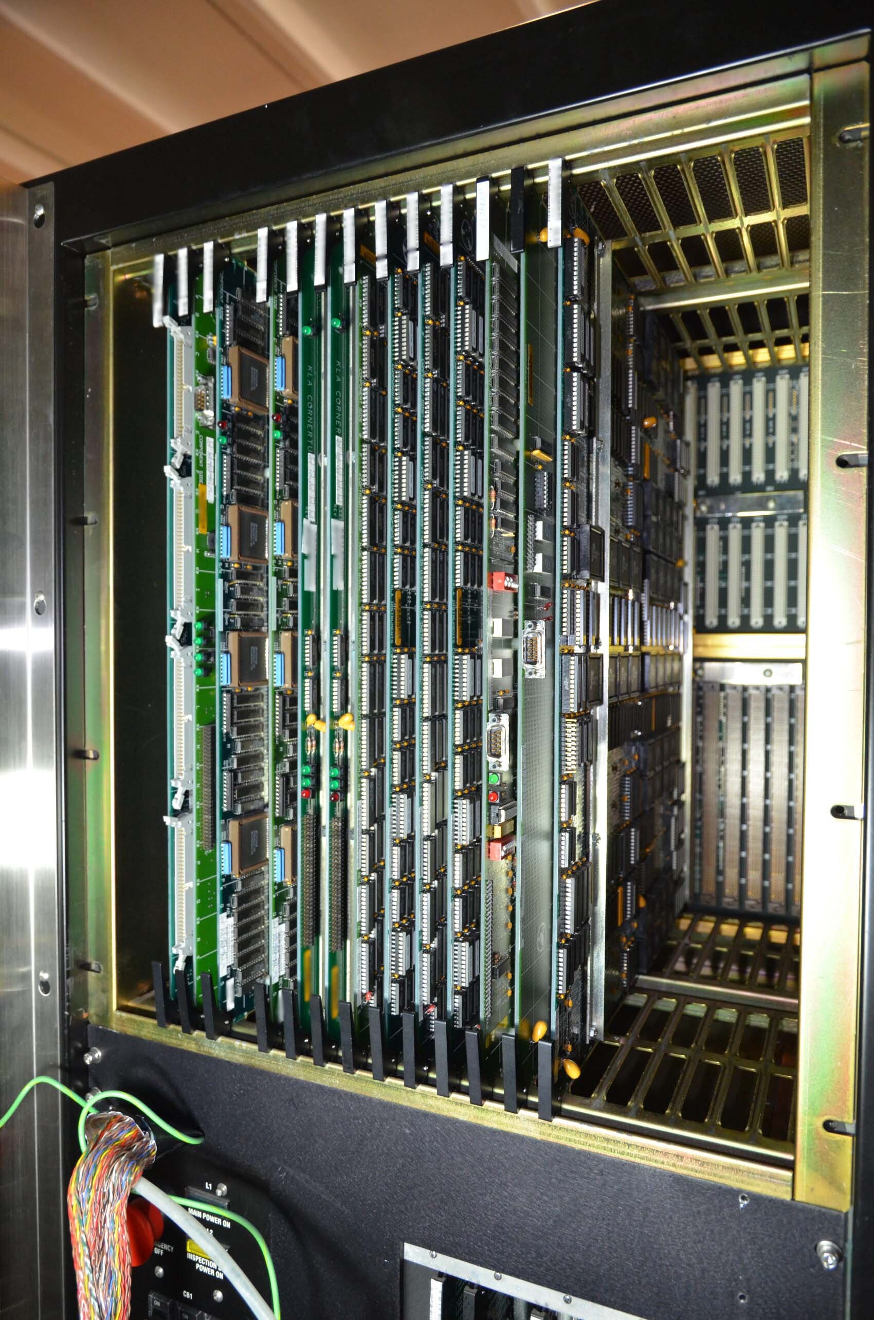

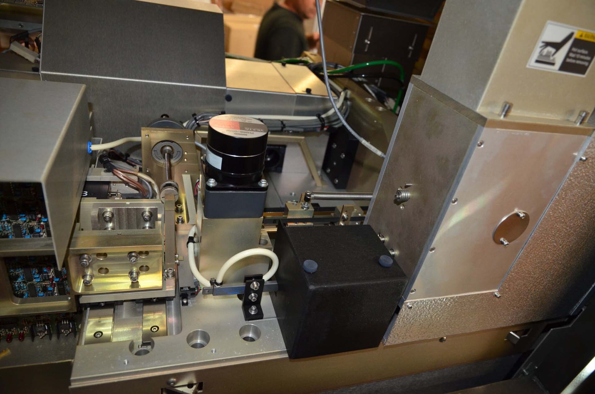

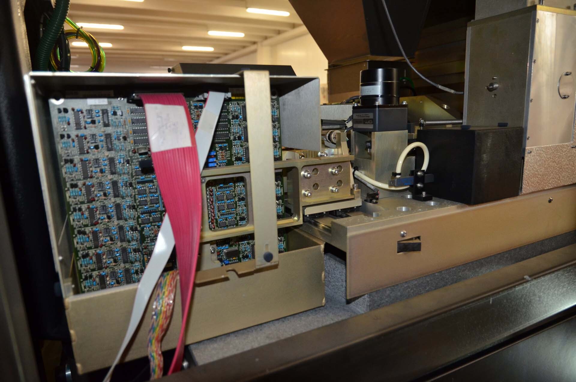

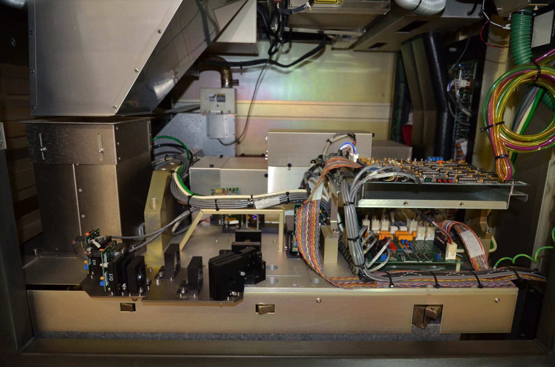

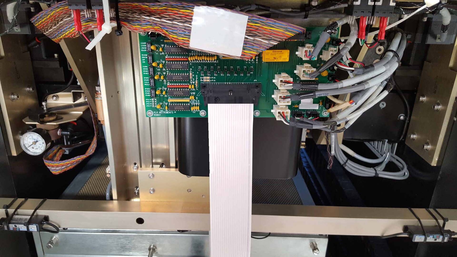


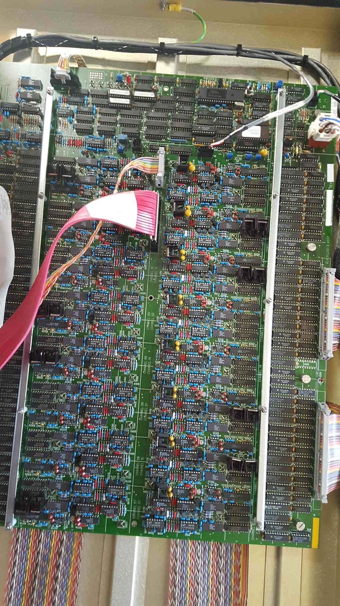


ID: 293644919
Wafer Size: 8"
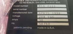
Vintage: 1996
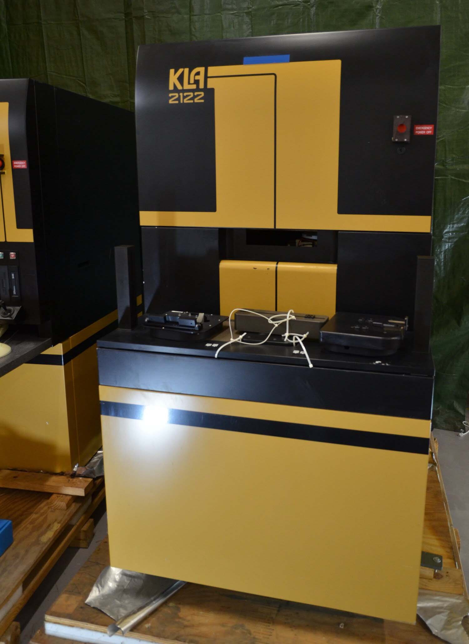
Wafer defect inspection system, 8"
Slots:
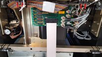
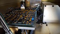
2 / 710-658086-20 Rev E0
3 / 710-658232-20 Rev H1
4 / 710-659412-00 Rev C0
6 / 710-659412-00 Rev C0
7 / 710-655651-20 Rev
8 / 710-655651-20 Rev
9 / 710-658172-20 Rev JI Y Interpolator, Phase 3
10 / 710-658177-20 Rev F1 X Interpolator, Phase 3
11 / 710-658172-20 Rev J1 Y Interpolator, Phase 3
12 / 710-658177-20 Rev F1 X Interpolator, Phase 3
13 / w024039
15 / 710-658036-20 Rev C3
Boards (Aux card cage):
Slots:
1 / 710-659465-20
3 / 710-650099-20 Rev L0 KLA DP Assy
6 / 710-650044-20 Rev D1
7 / 710-658363-20 Rev C0
1996 vintage.
KLA / TENCOR 2122 is a mask and wafer inspection equipment that utilizes a combination of automated and manual processes to accurately evaluate defects and variations in materials used in the production of integrated circuit components. KLA 2122 system has the capability to measure, detect and analyze variations in thin-film thickness levels, mask defects, wafer topography and electrical characteristics of the inspected material. It utilizes both optical and electrical microscopy for highly precise and reliable analysis of the material inspected at a sub-micron level, thereby promoting accuracy in detection and identification of defects. With its advanced imaging mode and spectroscopy capabilities, this unit features a high level of accuracy in measurement and evaluation, with a resolution size of 200 nanometers and a minimum sensitivity threshold of approximately 1 nanometer. The machine's handling flexibility is made possible by its integrated manipulation mechanism, designed to handle wafers of various sizes and materials, from 3 to 8 inches. This feature enables variability in approach, optimizing the inspection process to match different production requirements and product lifecycles. TENCOR 2122's software engine is built to handle both single- and multilayer thin-film imaging and analysis, delivering results with a very low defect-miss rate. Combined with the tool's multiple wafer geometric pattern analysis mode, it ensures a high-level of evaluation accuracy. In terms of speed, 2122 asset provides faster-than-standard throughput with its advanced imaging mode, allowing for decreased material consumption in the production line. As a result, the model reduces production cost, making it an invaluable time-saving device. In conclusion, KLA / TENCOR 2122 is a highly advanced mask and wafer inspection equipment suitable for a wide range of integrated circuits. It has the capability to measure and detect variations in thin-film thickness levels, mask defects, wafer topography and electrical characteristics of the inspected material, with an exceptionally high level of accuracy. Its fast imaging mode allows for faster-than-standard throughput, resulting in decreased material consumption and production cost. The system is a valuable time-saving device and provides cost-effective production quality assurance.
There are no reviews yet


