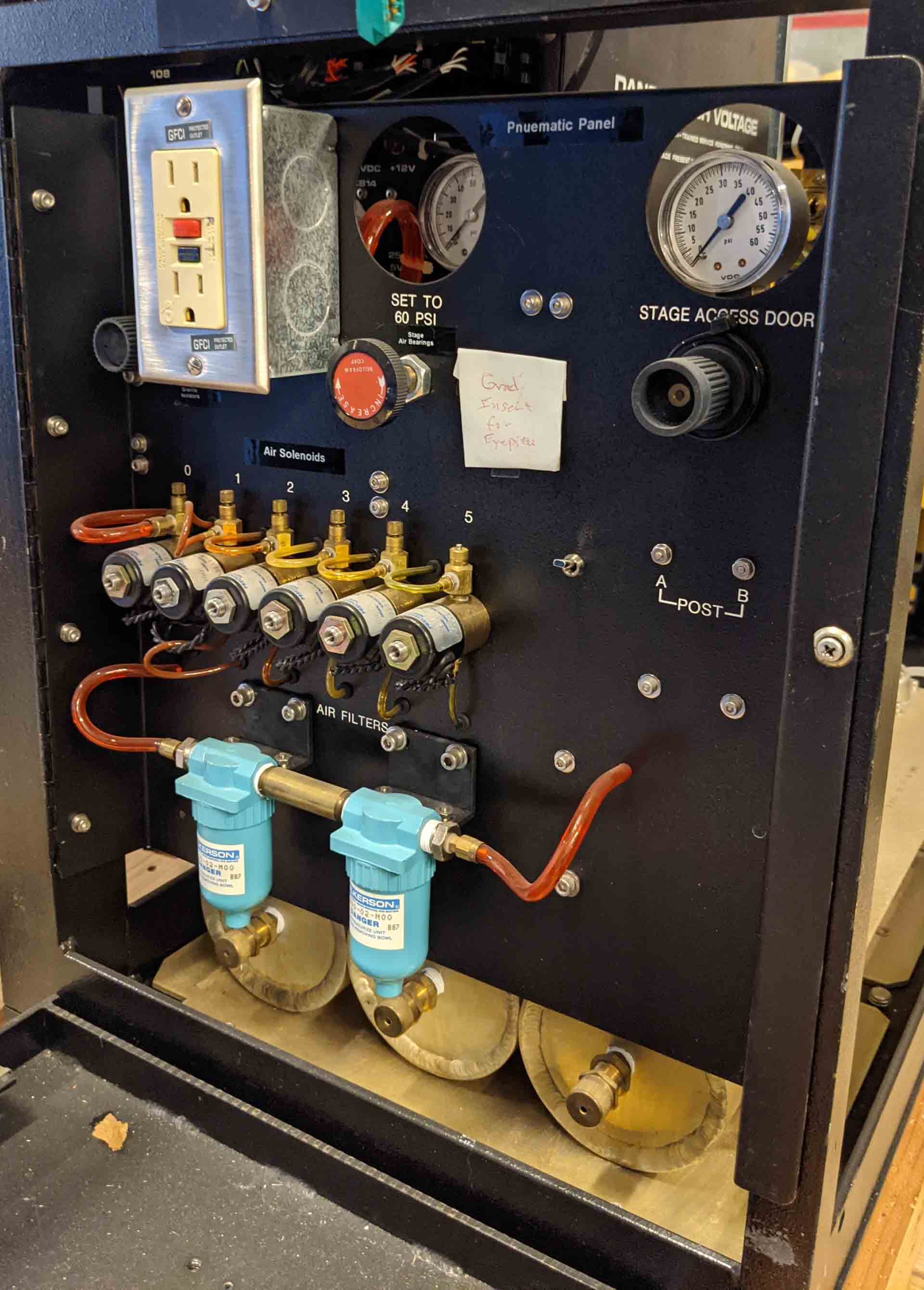
Used KLA / TENCOR 219 SWD #293635821 for sale
It looks like this item has already been sold. Check similar products below or contact us and our experienced team will find it for you.
Tap to zoom


Sold
KLA / TENCOR 219 SWD is an advanced mask and wafer inspection equipment engineered for quality assurance in semiconductor manufacturing. This multi-sensor system is capable of detecting defects on the nanometer level and handling wafer sizes up to 300mm. KLA 219 SWD is designed for inline applications and equipped with four brightfield and three darkfield optics. This allows it to detect sub-5nm defects on patterned silicon layers with a best-in-class sensitivity and throughput of 50 wafers per hour. An advanced proprietary Video Flex algorithm ensures more comprehensive and accurate inspection results. The unit features advanced imaging and metrology tools, such as KLA Image Navigation Machine (INKs) to achieve highest quality defect inspection, edge placement accuracy measurements, and advanced mask inspections. It is also equipped with advanced segmentation methodologies which allow it to distinguish real defects from false alarms. Additionally, wafer inspection parameters can be adjusted remotely and in real-time via the company's Global Remote Tool (GRS). TENCOR 219SWD has a touch-screen user interface which enables operators to easily switch between systems, adjust inspection parameters and view measurement data. The user interface also offers one-click button access to advanced automated defect review (ADR) and advanced imaging options, as well as automated edges placement accuracy measurements and customer-defined algorithms for customized inspection. 219SWD offers a variety of specialized smart inspection technology, such as surface defect detection, mask and wafer inspection, stress measurement and die-to-die inspection. It is built with safety and cleanliness in mind, and is suitable for 200, 300, and 450mm wafer sizes. Ultimately, KLA / TENCOR 219SWD is a technologically advanced, reliable inspection asset that offers best-in-class accuracy, repeatability, and efficiency when detecting defects on a nanometer level. Its wide range of features, automated functions, and user-friendly UI make it an ideal choice for quality assurance in the semiconductor industry.
There are no reviews yet