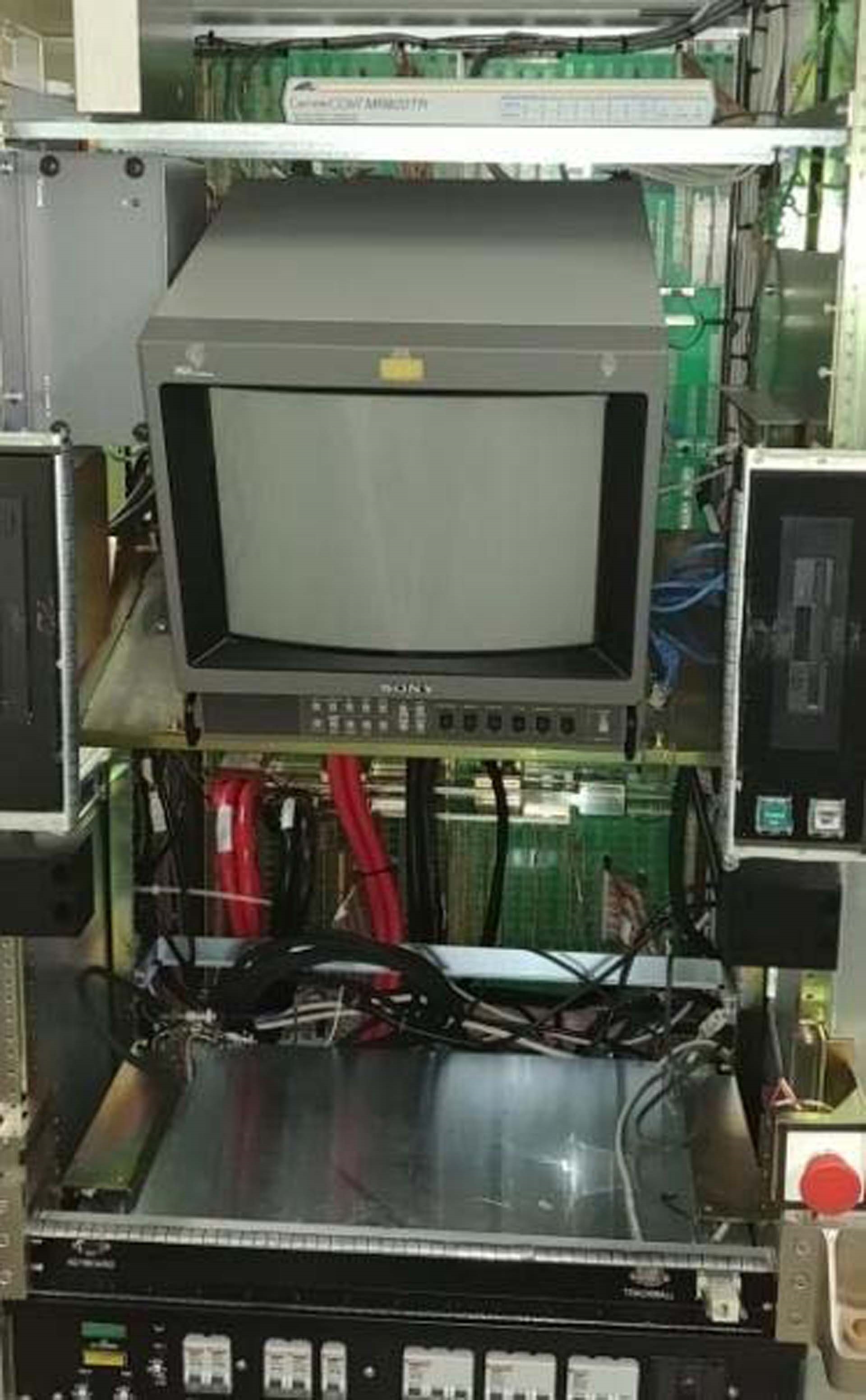
Used KLA / TENCOR 2350 #9270188 for sale
It looks like this item has already been sold. Check similar products below or contact us and our experienced team will find it for you.
Tap to zoom


Sold
ID: 9270188
Wafer Size: 8"-12"
Vintage: 2001
High-resolution imaging inspection system, 8"-12"
Dual open EFEM, 8"
GEM SECS and HSMS
Signal light towers: (4) Colors (R, Y, G, B)
Xenon lamp: 150 W
Wavelength illumination: 370~720 nm
Wavelength band: Visible, UV, I-line
Pixel size: 160~250 nm
User interface:
Monitor
Wafer display
Industrial PC (IPC)
Image computer (IMCs)
(48) IMC Boards
Does not include MM2S Board
Inspection station:
Granite suspension: Power
Cooling stage
Pneumatics optics plate
Air filter
Wafer handler (EFEM):
Dual open, 8"-12"
Dual SMIF, 8"
Dual FIMS, 8"-12"
Missing parts:
Lower monitor
Hard Disk Drive (HDD)
Power supply: 5 V
Keyboard, mouse and joystick
Solenoid board with valve
AF LED 1 Board
LP2 Cover
Y1 Flex board
(2) FVPA Boards
Robot controller
Fan Filter Unit (FFU)
UI and IS connecting cable
RGB Cable
RS232 Cable
Joystick cable
EMO Cable
(4) IMACS to UI Cables
(2) AZP FFA Cables
MIB Cable
Digital camera cable
2001 vintage.
KLA / TENCOR 2350 is a highly advanced mask and wafer inspection equipment, designed for semiconductor device manufacturing. It combines several technologies and techniques for imaging, visualizing, and characterizing defects automatically, in order to quickly locate and identify the smallest particles of contaminants and damage on the surfaces of semiconductor devices. KLA 2350 optics system uses dual-light source coherent illumination and high dynamic range imaging to reduce the need for manual inspection and create optimized visuals of the surface and features. It is also capable of automatically adapting to various wafer substrates, allowing it to capture high-resolution images regardless of orientation and size. Additionally, its interference microscope imaging unit is capable of 4X magnification for highly detailed data capture and analysis. KLA proprietary Multi-Command Vector Processor (MCVP) is used to evaluate the captured images in real time and search for localized defects, which are then segmented and identified by the machine. This principle of direct local defect detection reduces the overall data size, allowing quicker and more accurate analysis relative to the traditional SEM/EDS-based tool. It is also compatible with a large range of sample types, making it further applicable to a wide variety of applications. Furthermore, TENCOR Contamination Area Mapping (CAM) feature integrates fully with TENCOR 2350 analysis capabilities to detect and survey gross defects on a wafer, providing users with meaningful information and reducing inspection time and cost. The asset is also FIPS Compliant, so all data is protected from unauthorized access according to government standards. Overall, 2350 is an intelligent, high performance surface material inspection model designed to detect and examine even the smallest defects in an efficient manner. With its combination of powerful optics and high-grade analysis technologies, the equipment provides the accuracy and data needed for production and research tasks.
There are no reviews yet