Used KLA / TENCOR 2367 #293817504 for sale
URL successfully copied!

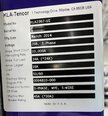
Tap to zoom
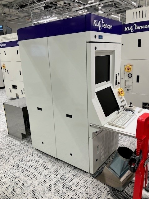

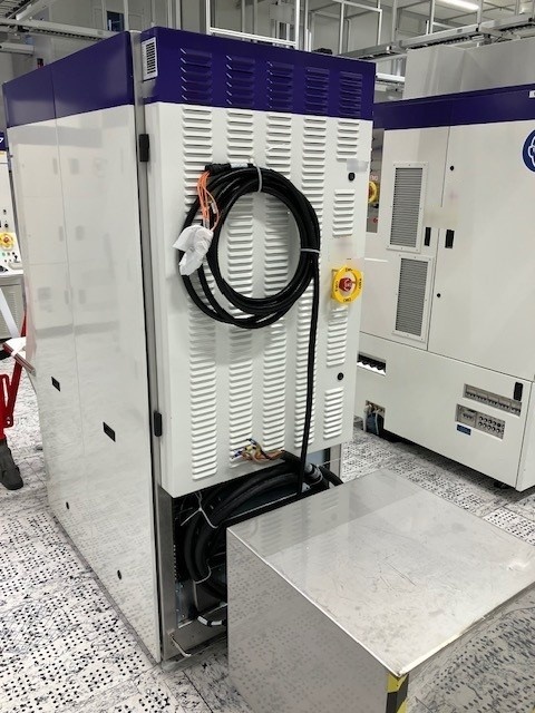
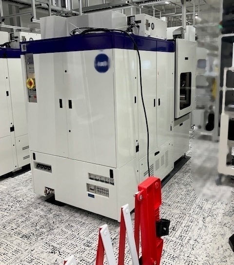
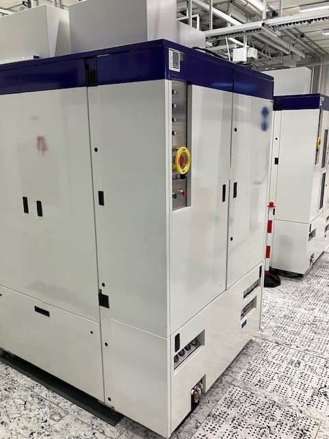
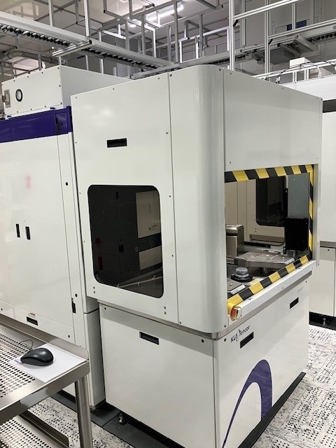
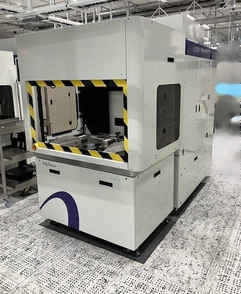
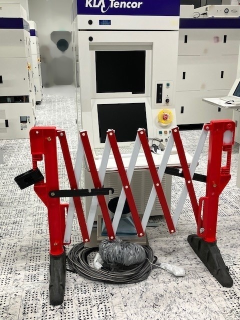
ID: 293817504
Wafer Size: 8"-12"
Vintage: 2014
Inspection system, 8"-12"
No laser
Robot
2014 vintage.
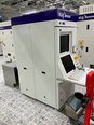
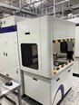
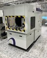
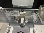
KLA / TENCOR 2367 Mask & Wafer Inspection equipment is a high-precision, automated wafer and photomask metrology and inspection system specifically designed for semiconductor manufacturing applications. The unit provides a fast, reliable solution for inspecting photomask and bare silicon wafer surfaces on production lines. KLA 2367 machine utilizes advanced inkjet technology to deposit an array of Ultraviolet (UV) fluorescent inspects on a photomask or wafer. These markers are then illuminated by a hyperspectral light source which generates a fringe pattern that is imaged by a complementary charge-coupled device (CCD) array camera.The fringe pattern is used to estimate the surface profile of the photomask or wafer and is compared against a user-defined specification. The tool then uses software algorithms to process and analyze the data to detect any surface anomalies or features. TENCOR 2367 Mask & Wafer Inspection asset has several benefits that help to improve the accuracy and productivity of semiconductor production. The model consists of multiple CCD cameras that are arranged to provide an optimal field of view coverage and depth of focus for mask pattern recognition. This ensures a higher accuracy of measurement. For wafer inspection, the equipment uses UV spectroscopy to detect wafer flatness, warp, pinspotting, and step height. The system is programmed to detect common flaws such as line breaks, gate bridging, and oxide nodules. Additionally, the optional automation option allows the unit to automatically match the positions of the wafers or masks relative to the light source for accurate inspection. 2367 Mask & Wafer Inspection machine is an advanced, productivity-enhancing solution that allows semiconductor manufacturers to reduce their overall inspection costs while ensuring quality control of their products. The tool's powerful software algorithms provide true 3D analysis of wafers and photomasks to provide highly accurate results. Additionally, it can be configured with an optional automation module to improve workflow and increase production throughput.
There are no reviews yet