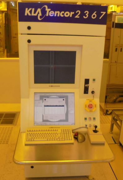
Used KLA / TENCOR 2367 #9189551 for sale
It looks like this item has already been sold. Check similar products below or contact us and our experienced team will find it for you.
Tap to zoom


Sold
ID: 9189551
Wafer Size: 12"
Vintage: 2007
Patterned wafer inspection system, 12"
Wafer calibration kit including DSW & shiny
Hardware options:
Hermos (2 CID devices)
Advantag (2 CID devices)
KEYENCE BCR Singlewire (2 CID devices)
Interlocks:
Safety Interlock for open panel
Safety Interlock for lamp
Exhaust:
600 ft3/min
100 ft3/min
1300 ft3/min
Integrated mini-environment
FEC Computer system
Intel® Pentium® 4 CPU 3.00GHz
2GB Memory (RAM)
Dell computer system
Intel®Xeon™ CPU 3.4GHz
2.48GB Memory (RAM)
DVD ROM
Mouse
Keyboard
HSMS/GEM SEMI E37 Compliant ethernet interface:
HSMS (E5 / E30 / E37)
GEM/SECS Automation interface (E4 / E5 / E30)
SEMI E84
SEMI E116
Hokuyo sensors:
Overhead transport (OHT)
Remote guided vehicles (RGV/AGV)
Auto switch for dual use environments
Basic automation package: E39, E87, E90 (Carrier management/wafer tracking)
Advanced automation package: E40, E94 (Process job, control job)
Windows 2000 based operating system SP4
Spatial population analysis :
Power options:
Array segmentation
Patch images: 64x64
Pixelperfect
RBB
RBMT
Sensitivity tuner
NPA
Photo option:
FEM
PWQ
Interface:
Data transfer
DVD-R
Ethernet
Hardware optic :
BB Visible pixels (0.62 mm, 0.39 mm, and 0.25 mm)
BB / I-Line / G-Line UV pixels (0.20 mm, 0.16 mm, and 0.12 mm)
Edge contrastTM
1600 MPPS Image computer
Array and random modes
High mag review optics
Anti-blooming TDI
High resolution review camera
Facilities:
Power: 2V5W-N, 18KW
Vw: 25 in Hg
CDA: 5 Sft3/min
Missing parts:
(4) Image computer nodes
2007 vintage.
KLA / TENCOR 2367 is an efficient and high quality mask and wafer inspection equipment developed by KLA Corporation. KLA 2367 uses advanced technology to provide rapid detection of defects at the wafer level and mask level, as well as providing an informative analysis of results. This system includes a dual-beam laser projection unit that independently detects specifications on both sides of the mask, on which it produces a fast and accurate analysis of the mask patterns. Furthermore, TENCOR 2367 integrates a number of advanced optical methods, such as scatterometry, and has several automatic processes to ensure the accuracy and optimization of the inspection. 2367 provides high-resolution imaging of the wafer and reduces the time and cost associated with defect detection. Through varying the intensity levels on each pixel, it easily detects subtle defects- even tiny particles or thin lines in the mask image. It is also capable of detecting protruded or hidden patterns on the mask, sub-pixel defects, electrical and optical defects, overlay and overlay misalignments. Additionally, KLA / TENCOR 2367 machine can generate defect maps that identify mask patterns and areas of potential improvement. KLA 2367 tool also offers several features and options that enhance its functionality and effectiveness. For instance, it includes a powerful image processing software that can generate 3D volume data from SEM (scanning electron microscope) images. It also offers customizable measurement temperature settings to ensure accuracy with different wafers, as well as the ability to control dust detection area, UV laser intensity, exposure time, and more. Furthermore, it is compatible with various types of samples, such as wafers and masks, to ensure accurate, high-speed processing. In sum, TENCOR 2367 is an advanced mask and wafer inspection asset that uses state-of-the-art technology to detect and analyze defects. It offers fast and reliable detection results that can generate highly informative defect maps and images. It also includes a range of features that can be customized to ensure accuracy and precision. With its high-resolution imaging and image processing capabilities, 2367 is ideal for semiconductor and mask making industry.
There are no reviews yet