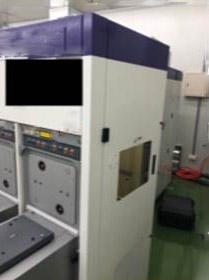
Used KLA / TENCOR 2367 #9276696 for sale
It looks like this item has already been sold. Check similar products below or contact us and our experienced team will find it for you.
Tap to zoom


Sold
ID: 9276696
Wafer Size: 12"
Vintage: 2007
Inspection system, 12"
Carrier ID readers
Operating system: Windows 2000 SP4
HSMS / GEM Semi E37 compliant ethernet interface:
HSMS (E5 / E30 / E37)
GEM/SECS Automation interface (E4 / E5 / E30)
SEMI E84
SEMI E116
Hokuyo sensors for use with:
Overhead transport (OHT)
Basic automation package: E39, E87, E90 (Carrier management / wafer tracking)
Advanced automation package E40. E94 (Process job, control job)
InlineADC
ITF
Load port UI
MDAT
Mixed mode
NFS Data transfer
Interface data transfer DVD-R ethernet
Spatial population analysis:
Power options
Array segmentation
Patch images: 64 x 64
Pixel perfect
RBB
RBMT
Sensitivity tuner
NPA
Hardware optic:
BB Visible pixels (0.62 mm, 0.39 mm, and 0.25 mm)
BB/I-Line/G-Line UV pixels (0.20 mm, 0.16 mm, and 0.12 mm)
Edge contrast
1600 MP PS Image computer
Array / Random modes
High mag review optics
Anti-blooming TDI
Review camera
2007 vintage.
KLA / TENCOR 2367 is a mask and wafer inspection equipment that is specifically designed for precise optical inspection of the die and substrates. KLA 2367 gives a detailed, comprehensive, and accurate inspection of substrates for defects, while providing extreme levels of repeatability and flexibility for many applications. The system is equipped with a 5MP sputter coated scientific-grade CCD camera for high resolution inspection. The camera has a field-of-view of 25.4/17.6 mm and it offers selectable imaging resolutions of 5, 2.5, 1.25 microns/pixel, as well as 1 micron/pixel transmissive mode capability. TENCOR 2367 also features a proprietary CMOS sensor technology that eliminates imaging distortion when examining fine features and geometry. This is enabled by a patented calibration-free technique that offers superb repeatability. 2367's patented alignment technology allows the unit to deliver extremely accurate inspection results. During each step of the inspection process, the sample under test is aligned to the inspection grids via a unique encoding mechanism. This ensures that data from each sample is precisely locatable under the imaging optics - irrespective of the sample's position in the machine. The built-in stitching algorithm provides a 'slide-and-stitch' function that allows the tool to make dynamic image mosaics while being compensated against stage non-linearity and non-symmetry. This means that data from various parts of the substrate, including reworked, eutectic, and die attach areas, can be more easily compared. KLA / TENCOR 2367 is designed for fast and efficient defect detection too. Using high-throughput motorized stages, the asset is capable of scanning entire substrates at a speed of up to 200mm/second. Furthermore, it supports the integration of various data output sources such as an EDA link to streamline defect-to-design data transfer. In conclusion, KLA 2367 is an ideal model for inspecting wafers and masks. Its combination of precision imaging, advanced alignment technology, and an efficient stitching algorithm ensure that users obtain the highest level of accuracy when examining substrates for defects.
There are no reviews yet