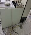
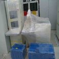
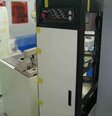
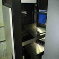
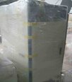
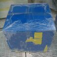
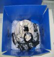
Used KLA / TENCOR 2608 #9386377 for sale
URL successfully copied!
Tap to zoom


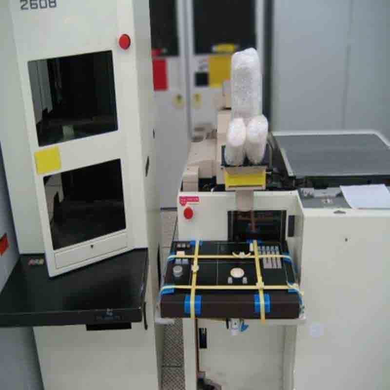

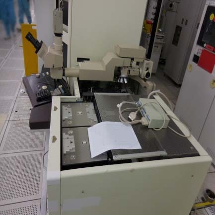

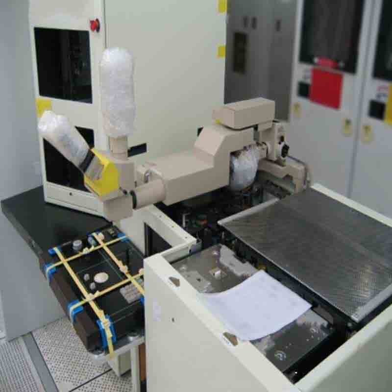


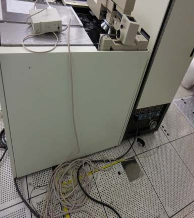


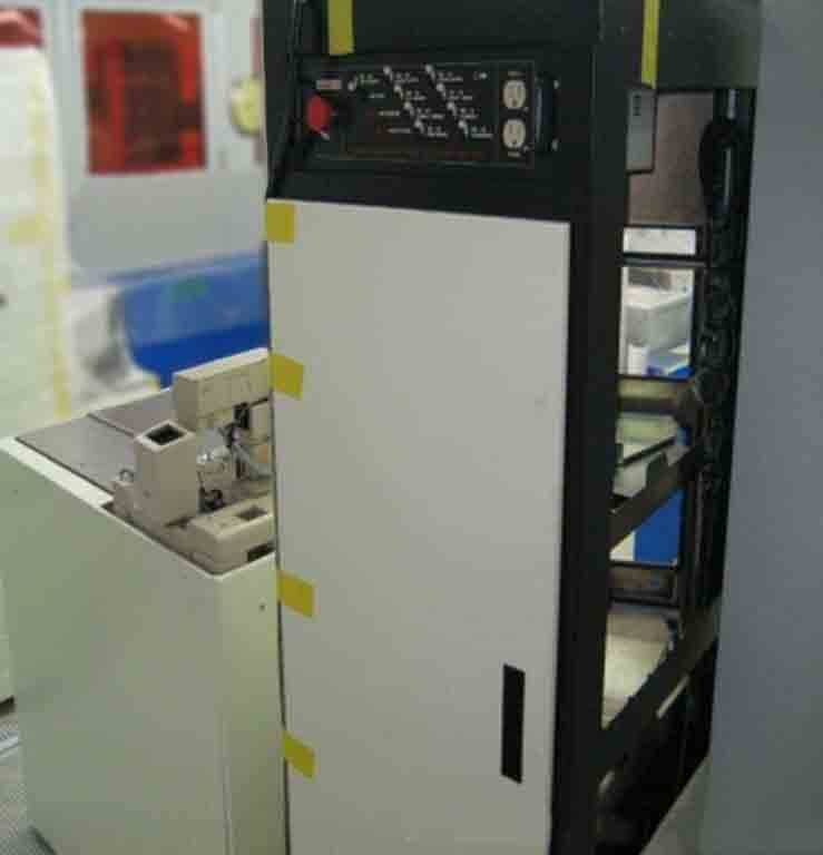




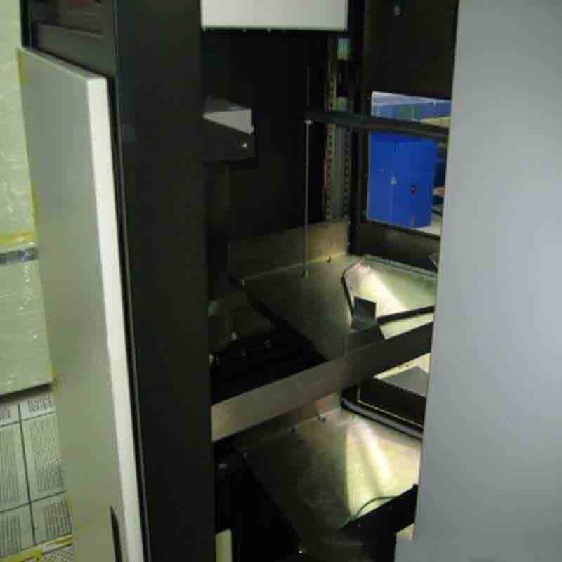






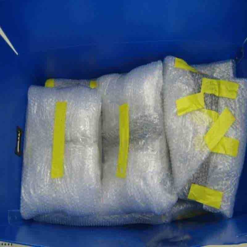

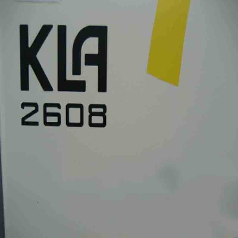

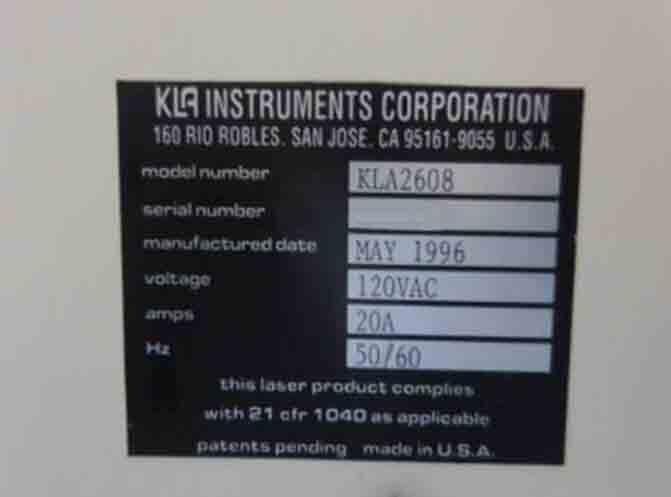

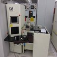
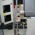
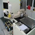
KLA / TENCOR 2608 Mask & Wafer Inspection Equipment is an automated wafer inspection and metrology platform suitable for advanced process control and line monitoring of 200mm and 300mm wafers. The system is designed for accurate measurements of critical features on photomasks, semiconductor wafers, and flat panel displays. Its large field of view, nanometer resolution, and high throughput capabilities make it an ideal solution for wafer and mask lithography control. KLA 2608 includes a sensitive color CCD line scan imaging sensor, high-performance optics, and high-resolution wafer stage. The CCD line scan imaging sensor features a pixel size of less than 8µm, allowing for high-resolution images of defects on the mask and wafer surfaces. In addition, TENCOR 2608 offers a large field of view of 4 x 3 inches, providing an expansive overview of the sample, enabling precise identification and targeting of defects. 2608 is capable of performing various measurements on mask and wafer surfaces, such as film thickness, refractive index, topography, overlay verification, line widths, line and space measurements, capturing line breaks, handling dark line detection, and verifying wide lines. In addition, it offers specialized algorithms for automated defect detection and review, improving productivity and accuracy. KLA / TENCOR 2608 is equipped with a high-speed wafer transport unit that is capable of loading and unloading up to four wafers at a time, allowing for high-throughput capabilities. KLA 2608 also comes with an integrated process management software for automated job programming, remote access, centralized data management, and review. KLA 2608Mask & Wafer Inspection Machine offers enhanced accuracy, productivity, and repeatability for the inspection and metrology of semiconductor wafers and photomasks. Its powerful features, including the advanced CCD line scan imaging sensor, high-performance optics, 4 x3-inch field of view, nanometer resolution, and high-speed wafer transport capabilities are suitable for high-precision wafer and mask process control.
There are no reviews yet
