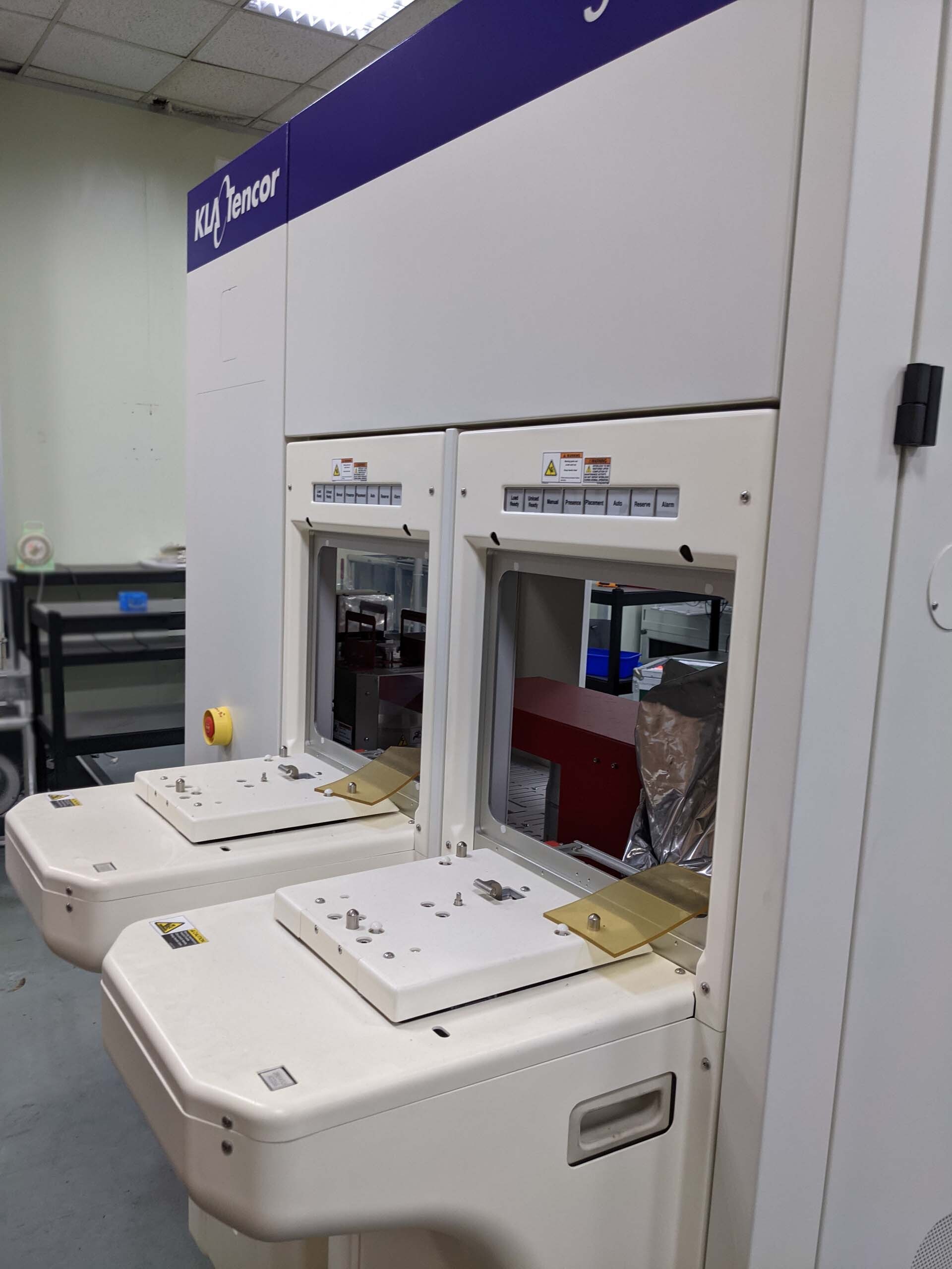
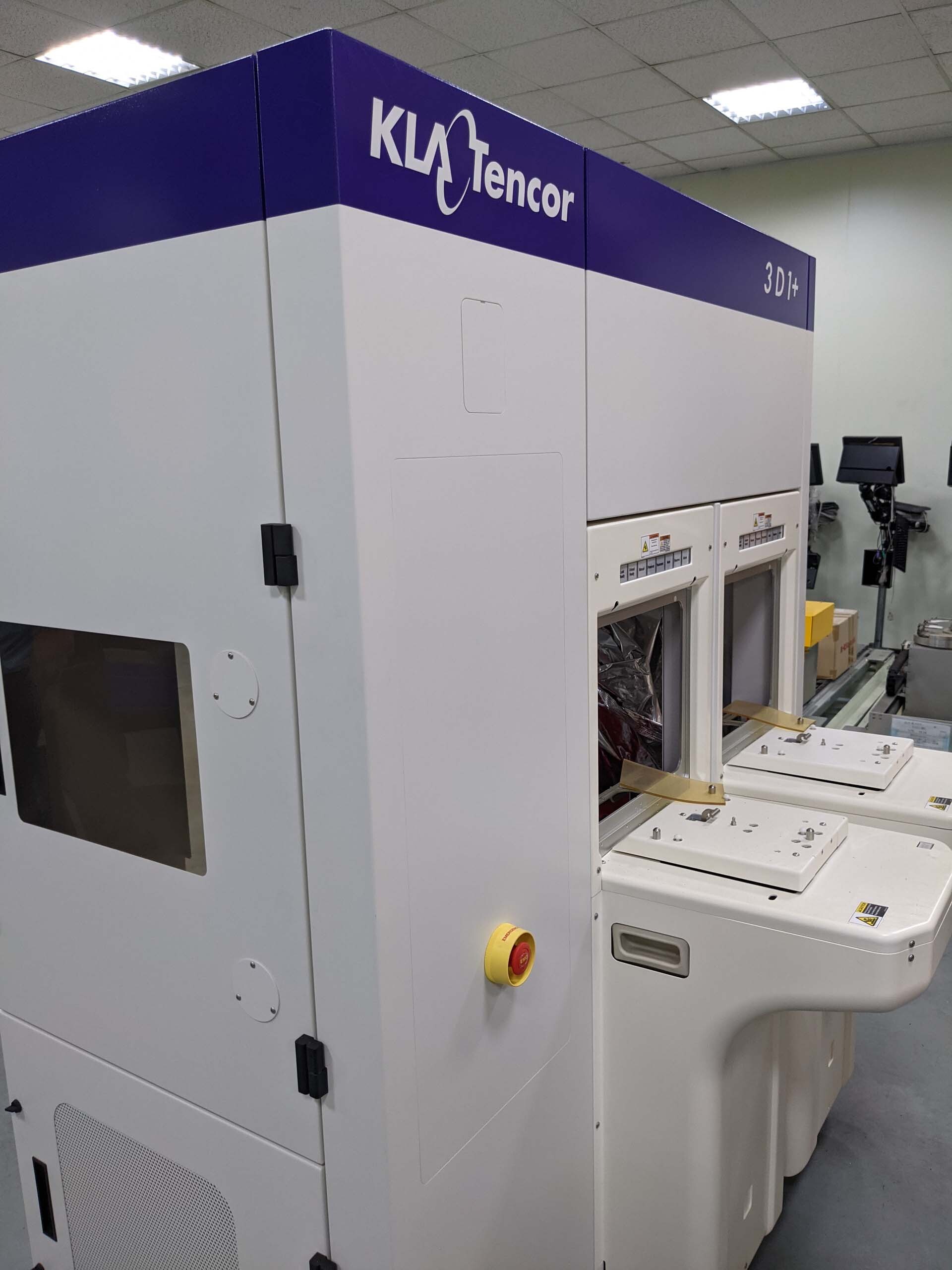
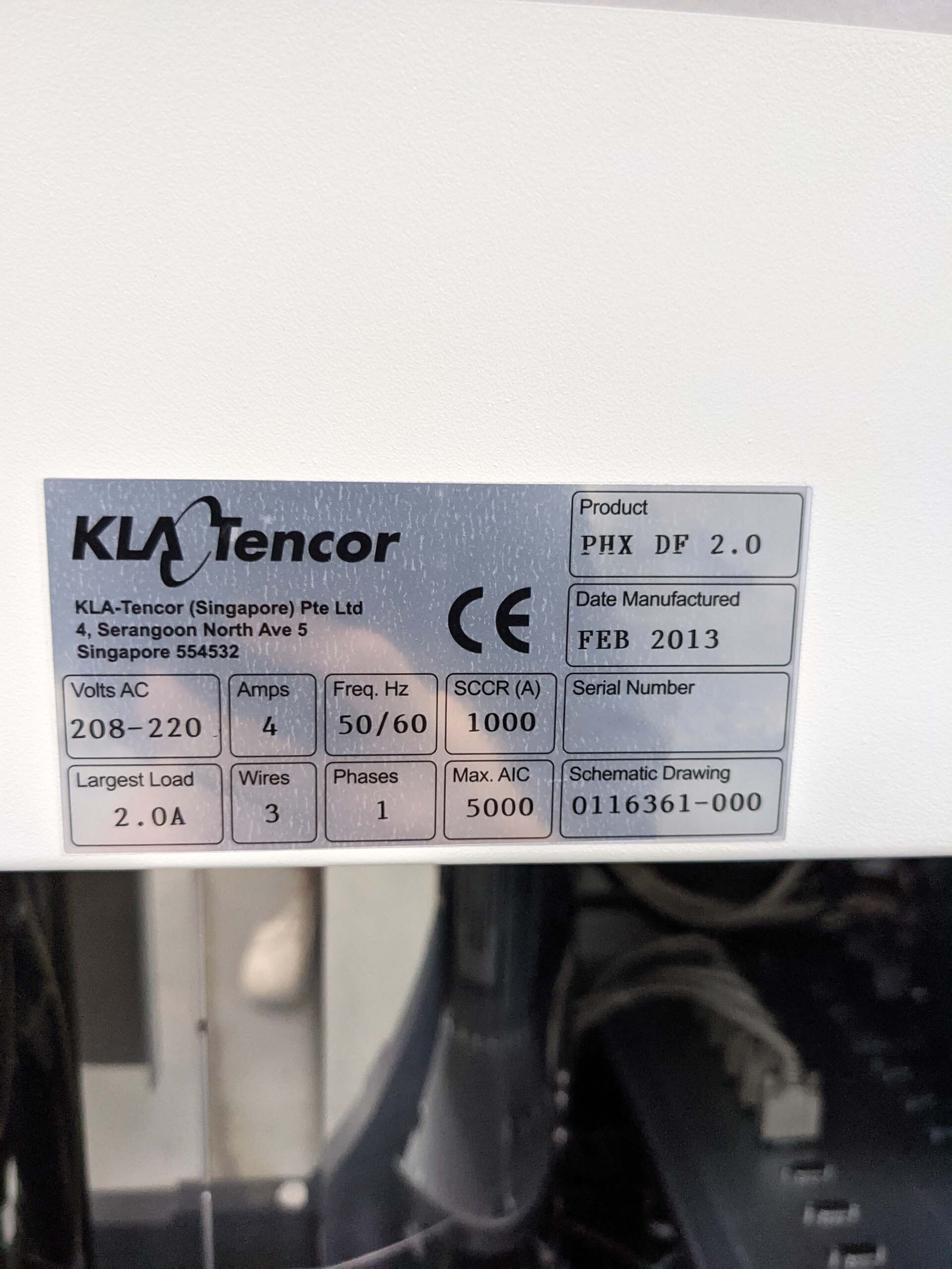
Used KLA / TENCOR 3Di #9384479 for sale
URL successfully copied!
Tap to zoom


ID: 9384479
Wafer Size: 12"
Vintage: 2013
System, 12"
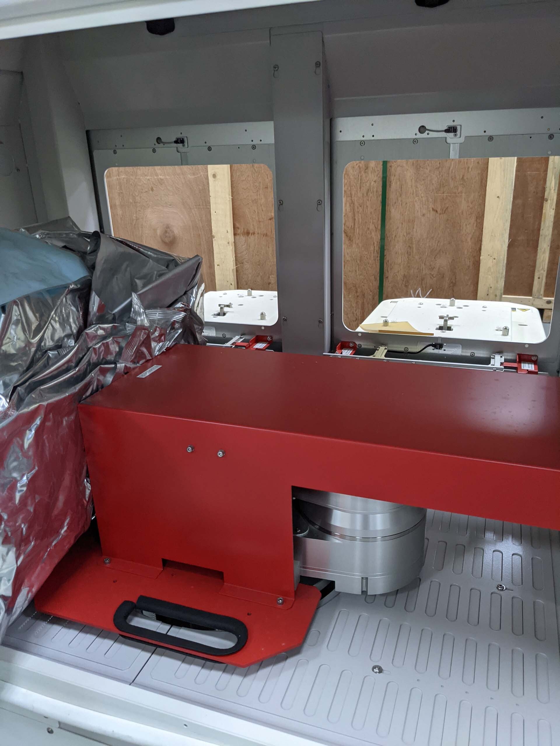
EFEM Module
YASKAWA Robot 9206
(2) SINFONIA Load ports
2013 vintage.
KLA / TENCOR 3Di is an advanced-generation mask and wafer inspection equipment that is designed to enable superior defect detection for high-speed manufacturing of integrated circuits. It features 3D imaging technology that uses height, color, brightfield, and darkfield information to detect microscopic flaws, as well as wafer-to-mask alignment capability to compare die to known patterns and detect discrepancies. KLA 3Di is equipped with a 5-megapixel detector allowing high resolution imaging of critical features, allowing for greater sensitivity in the detection of defect sources. It also provides powerful, specialized algorithms to analyze data quickly and accurately detect both parametric and non-parametric defects. The system is configured with advanced pixel binning capabilities to enable higher throughput without sacrificing defect sensitivity, compatibility with standard formats for automated defect inspection, and a data accumulation capability that stores inspected images and related wafer information for analysis and archival. TENCOR 3Di can detect defects on the order of sub-micron sizes in both 2D and 3D, with 3D profiles visualized in real-time or saved as a reference file for later analysis. It is able to identify missing, shifted, stretched, rotated, or otherwise misaligned features and layers. It can also extract needed data from the image such as topography, step heights, and contour lines. The unit is compatible with all current mask lithography systems, and its intuitive user interface allows operators to customize the inspection parameters, view raw wafer images, and analyze multiple defect types. It employs a compatible stage machine, making it easy to set up and quick to inspect what can otherwise be an extremely complex process. Finally, 3Di tool is equipped with intelligent auto-discovery algorithms that can detect subtle defects in advanced-node images, providing better yield and improved overall device quality. This enables faster time-to-market for finished devices.
There are no reviews yet


