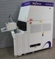
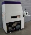
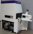
Used KLA / TENCOR Archer 200 AIM #9255571 for sale
URL successfully copied!
Tap to zoom
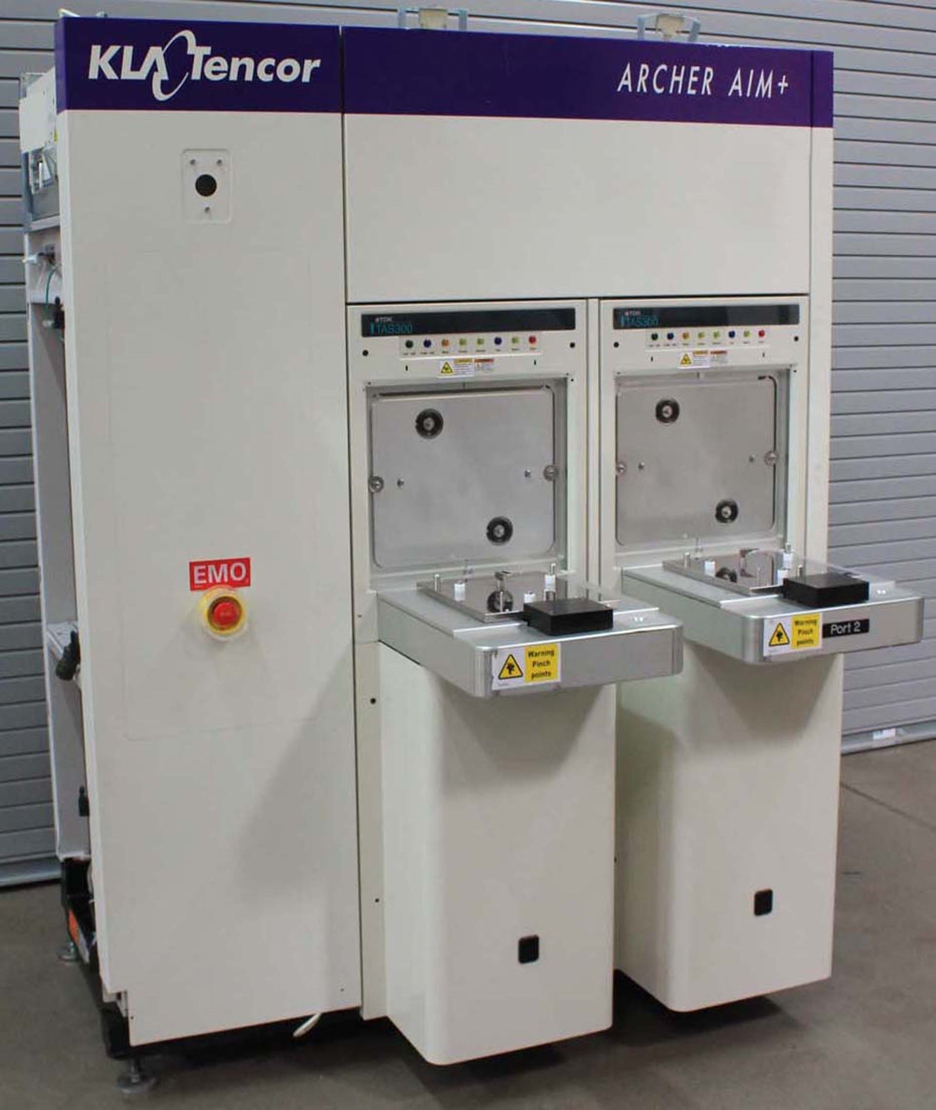

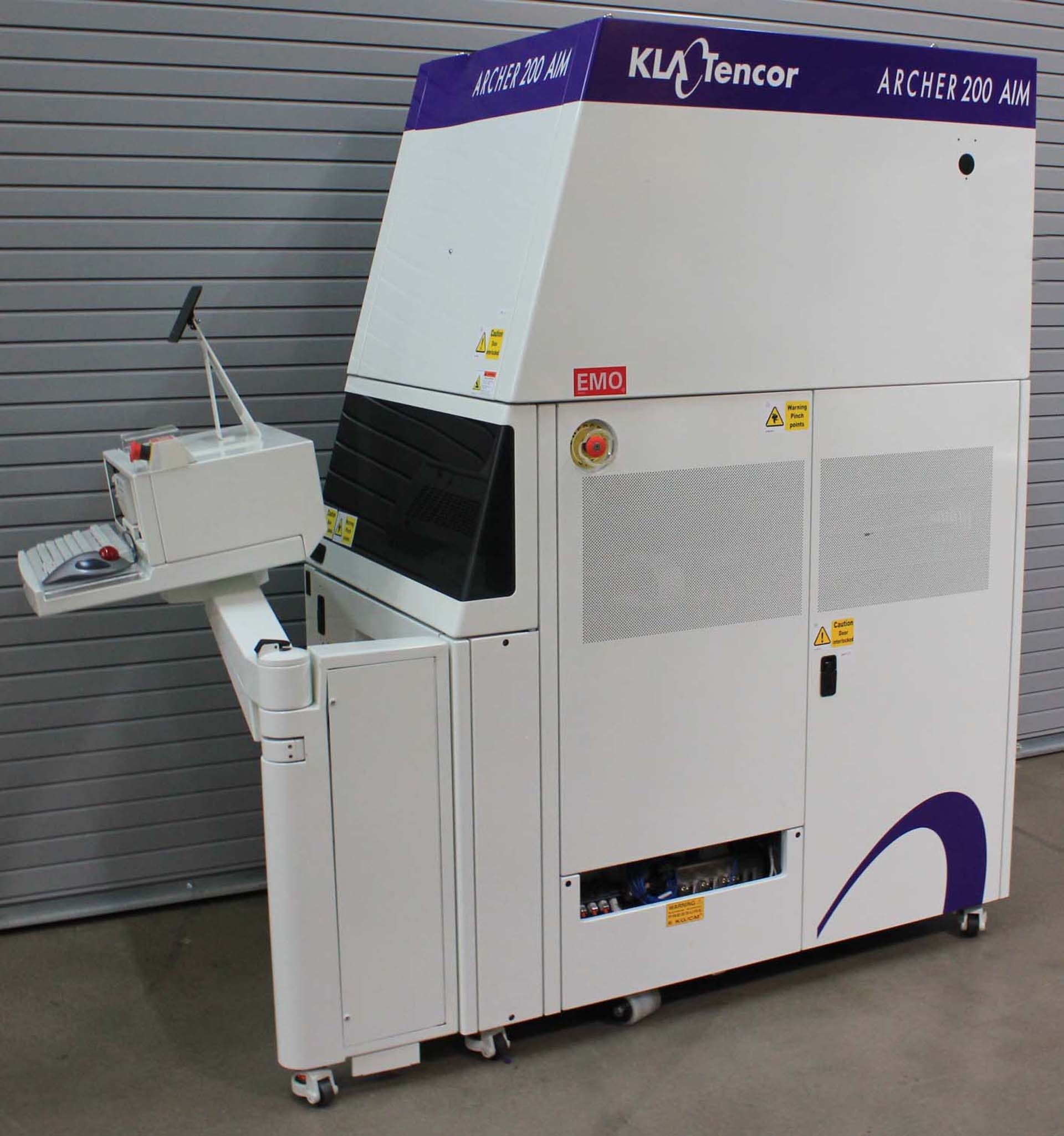

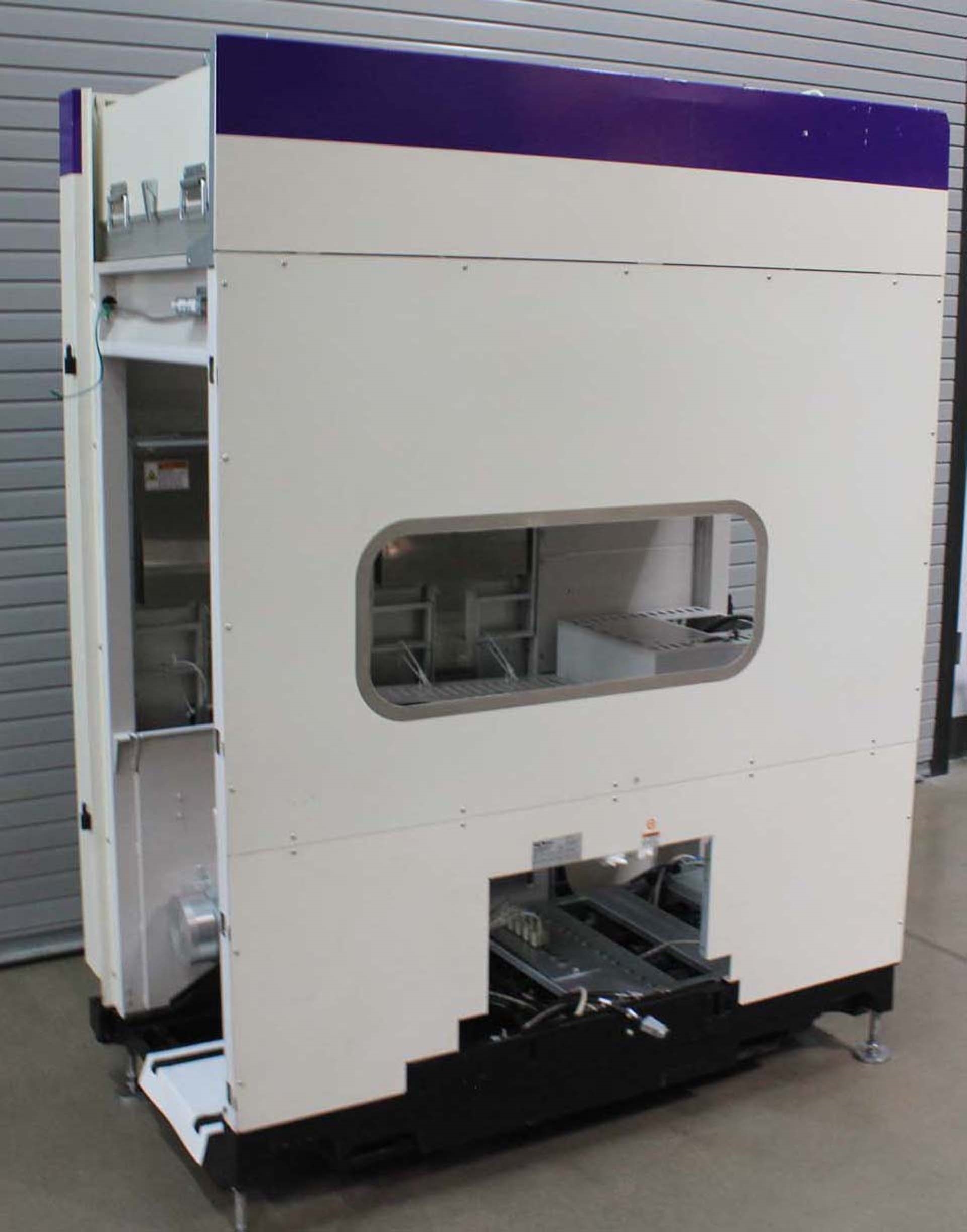

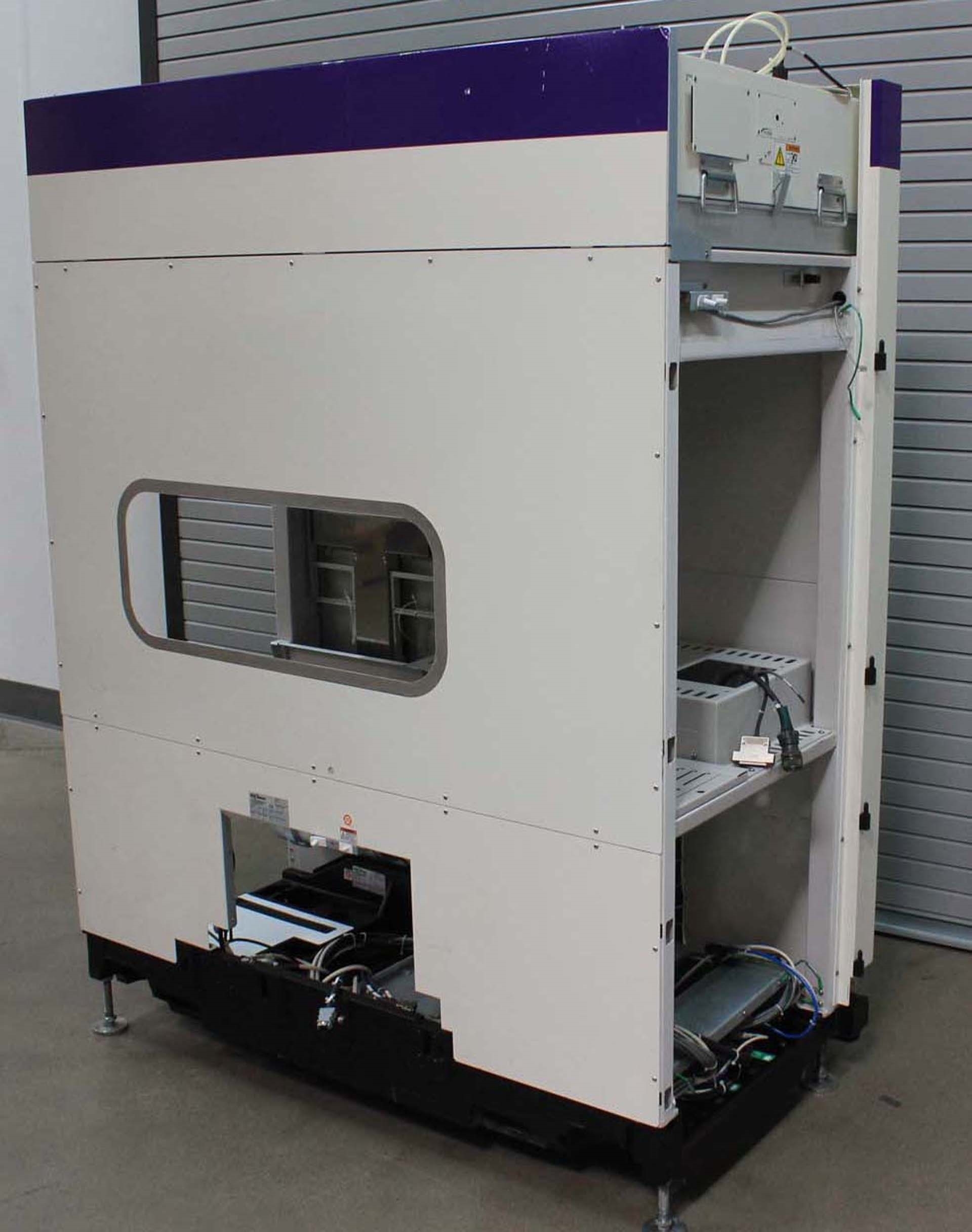

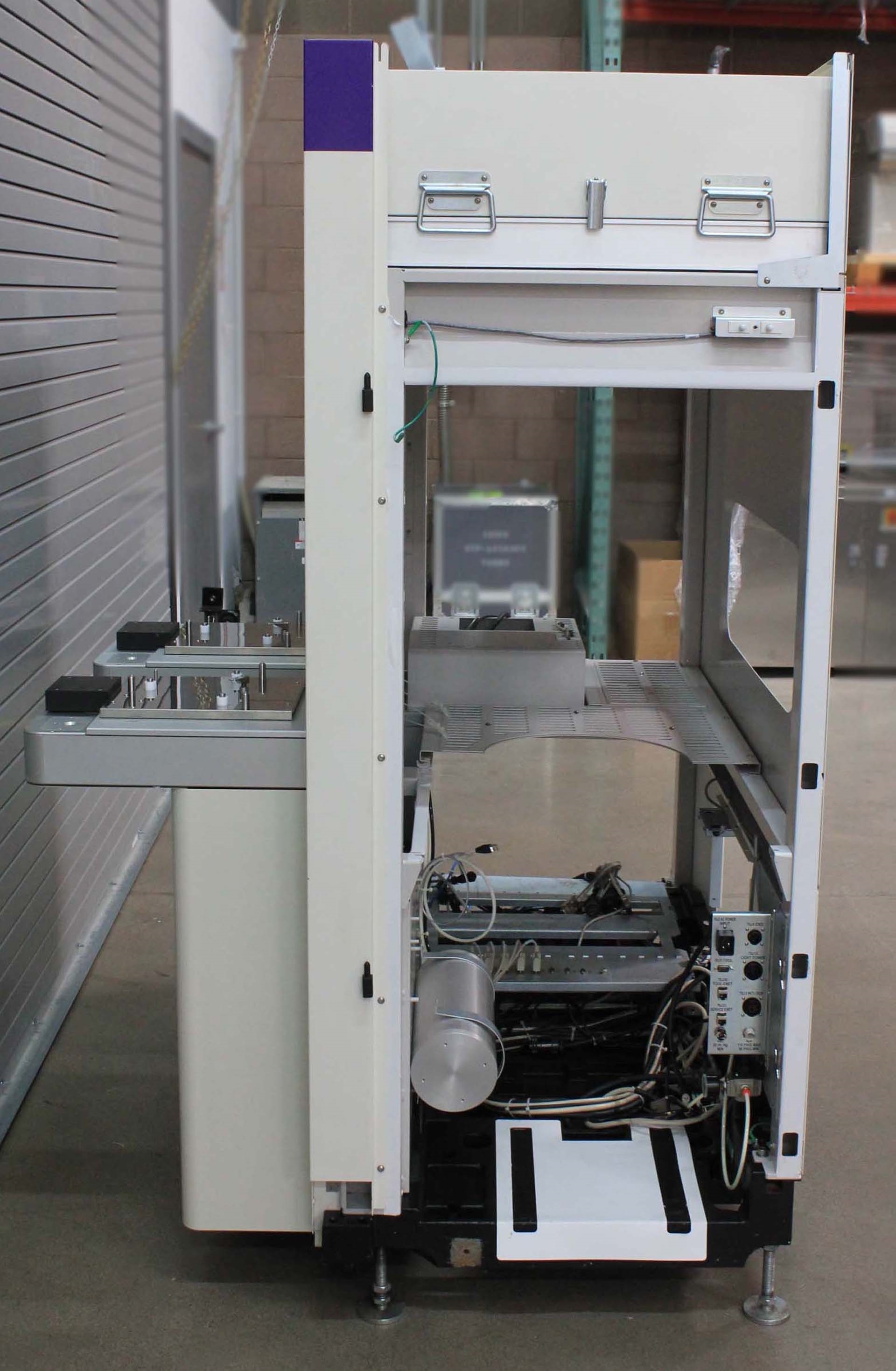

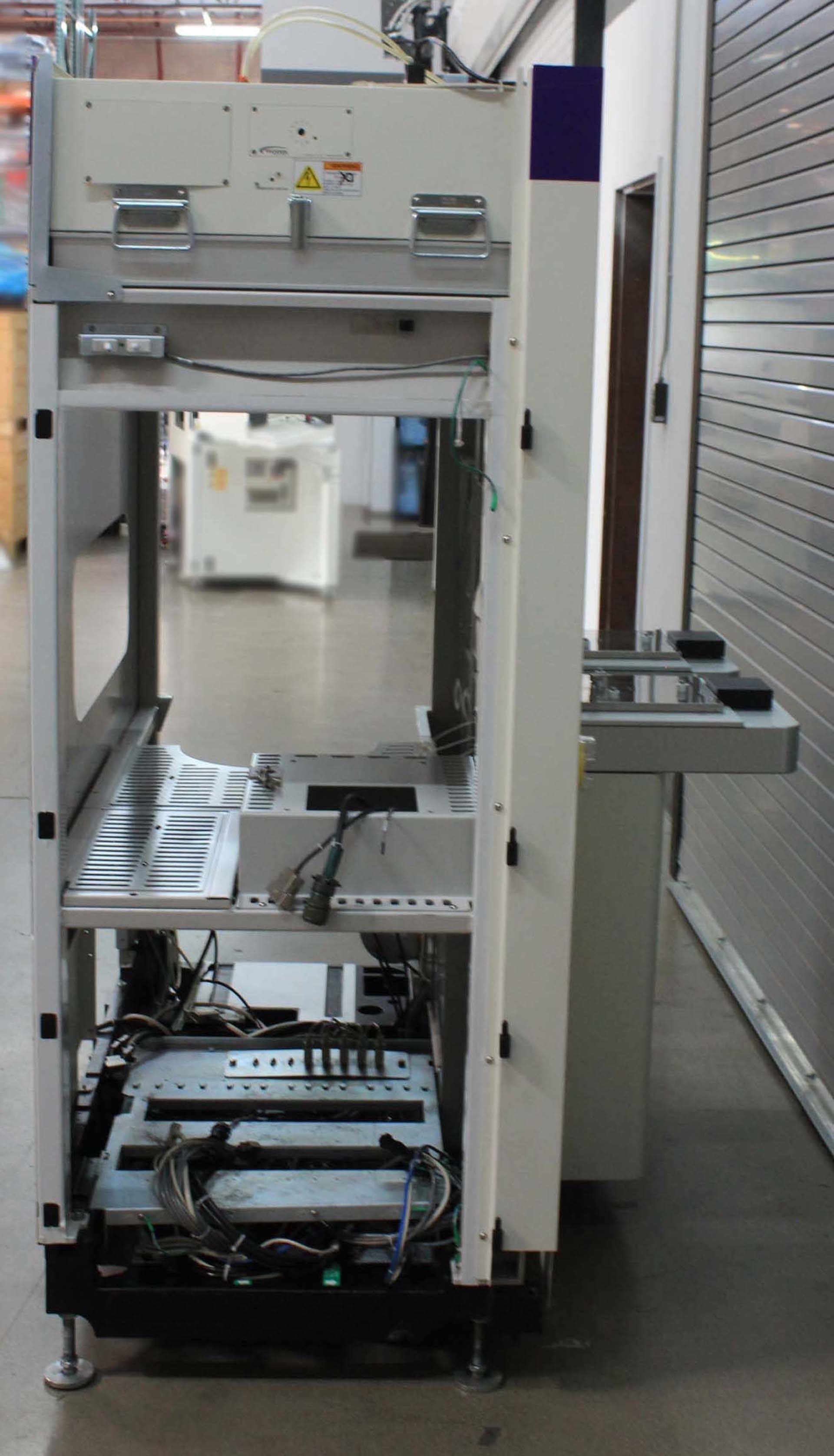

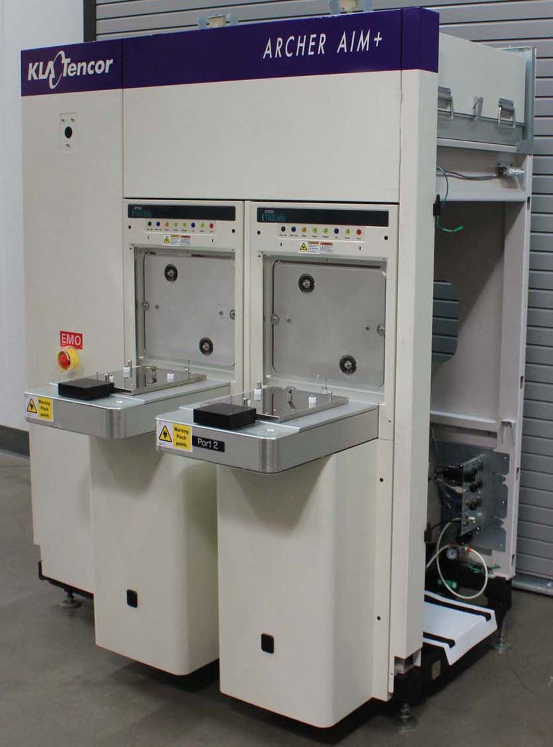

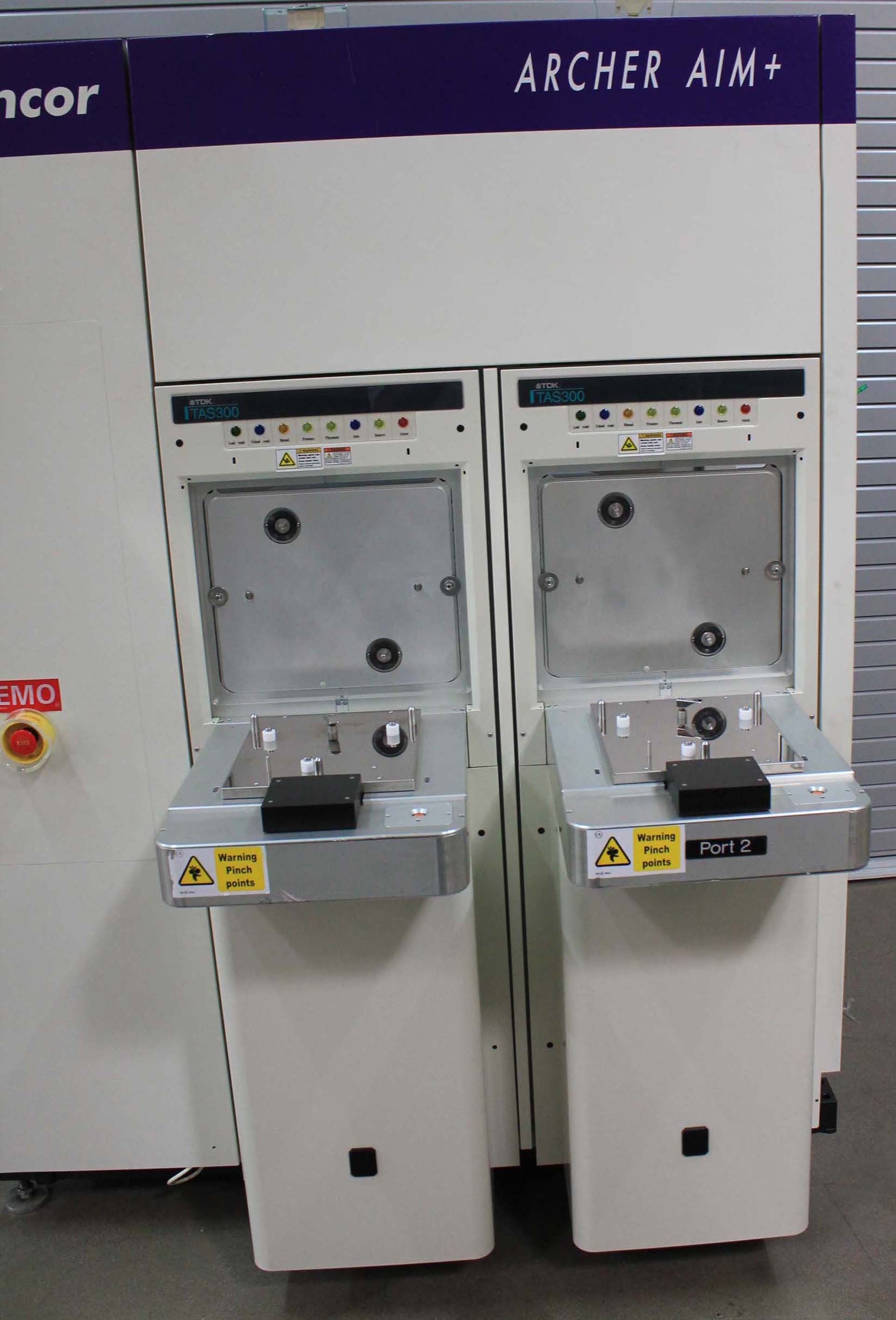

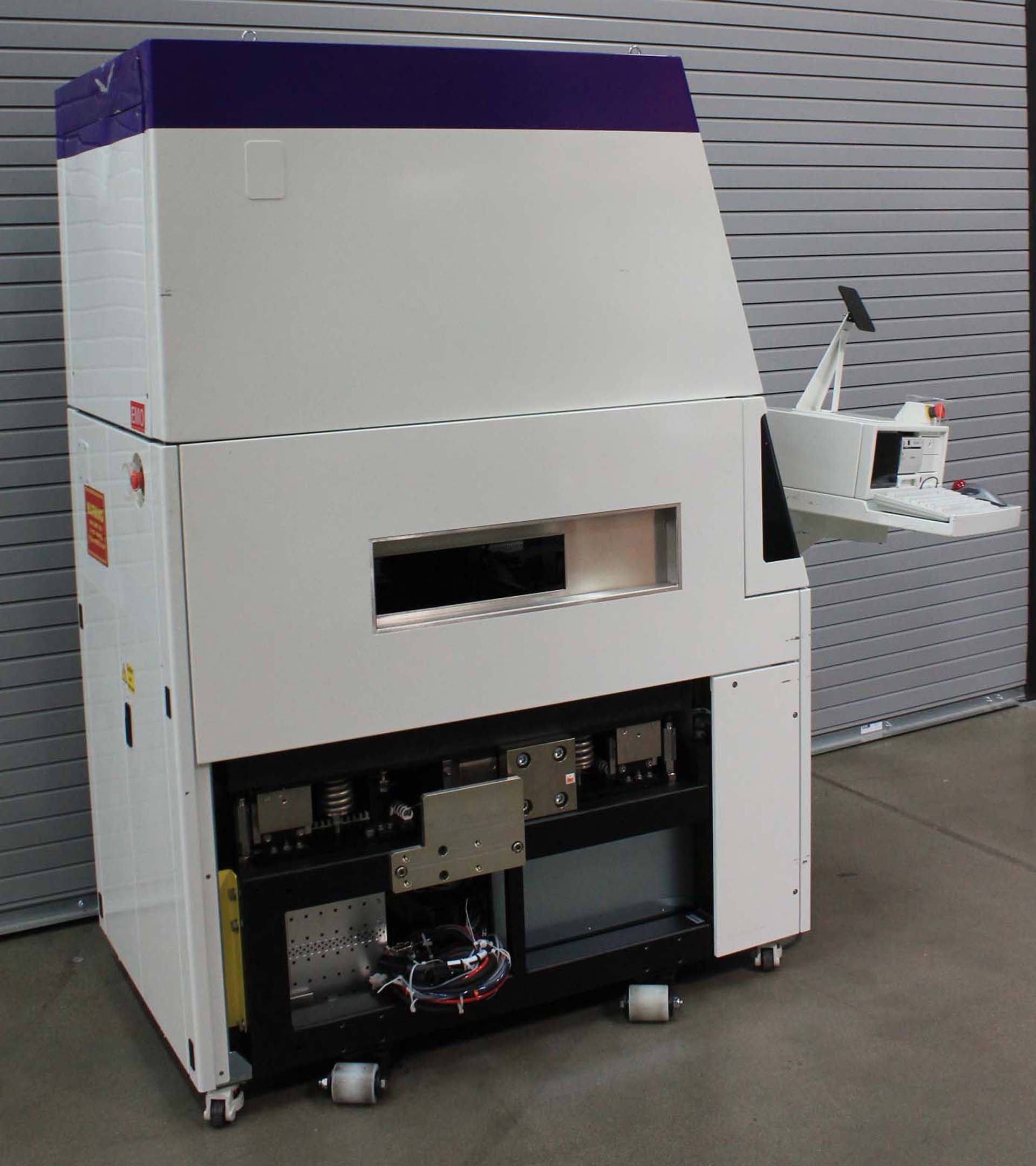

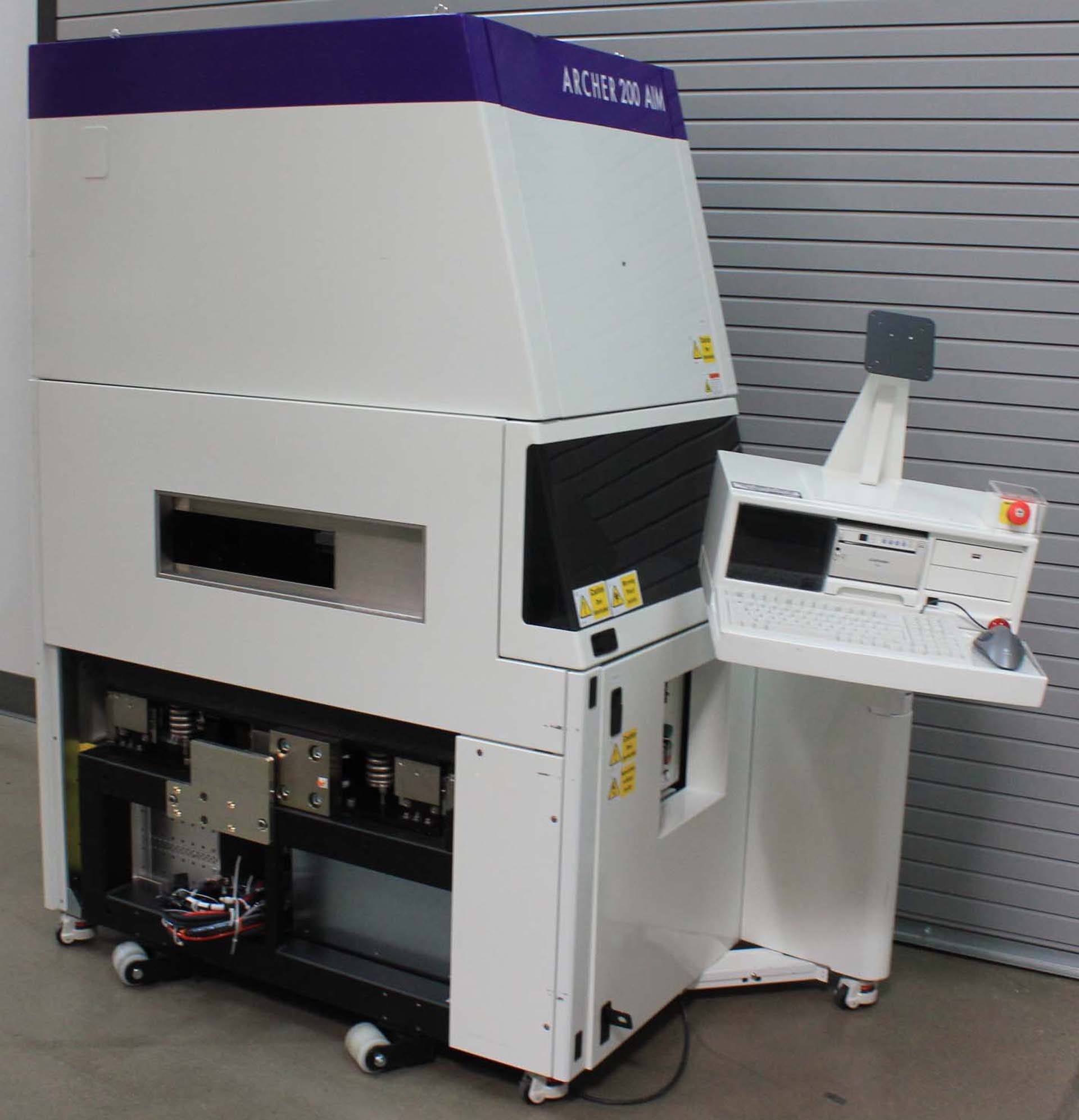

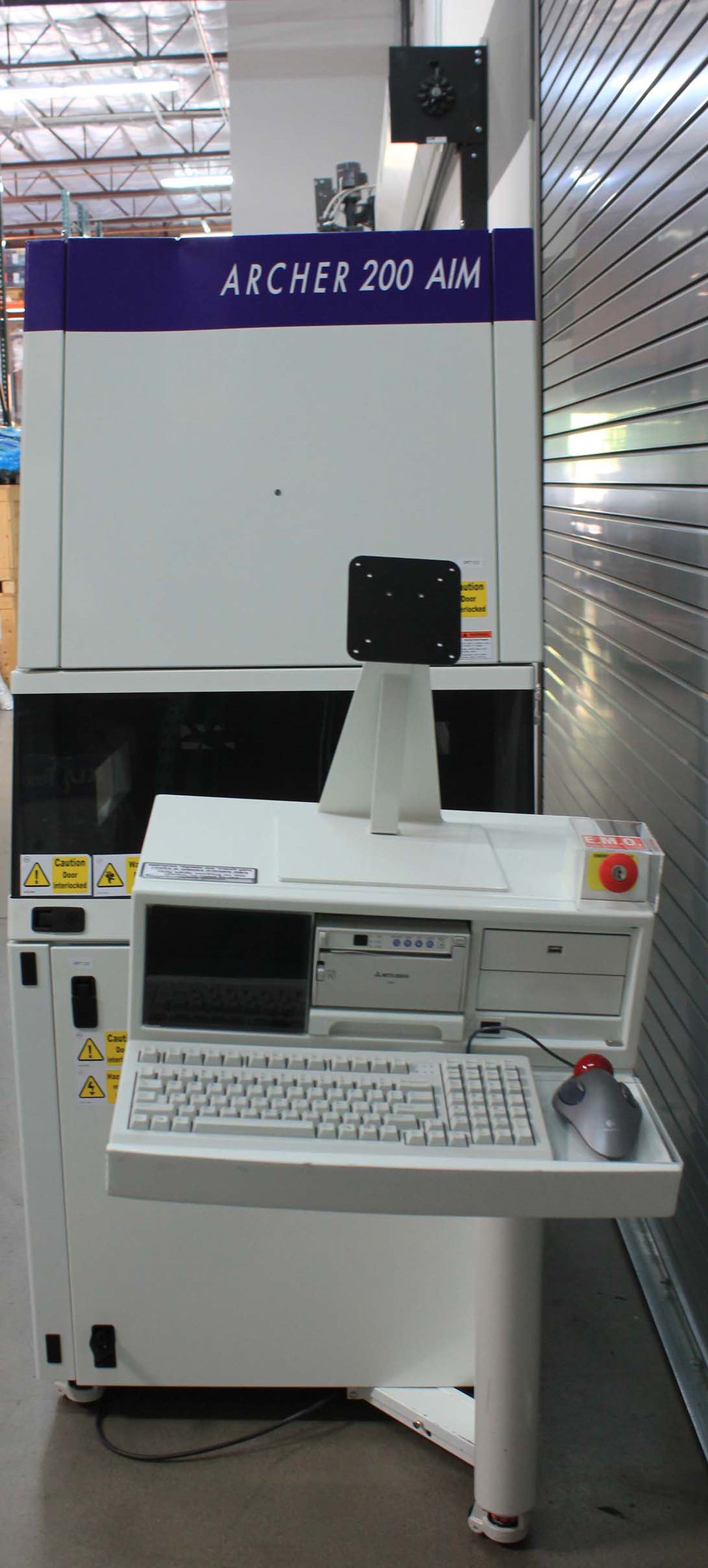

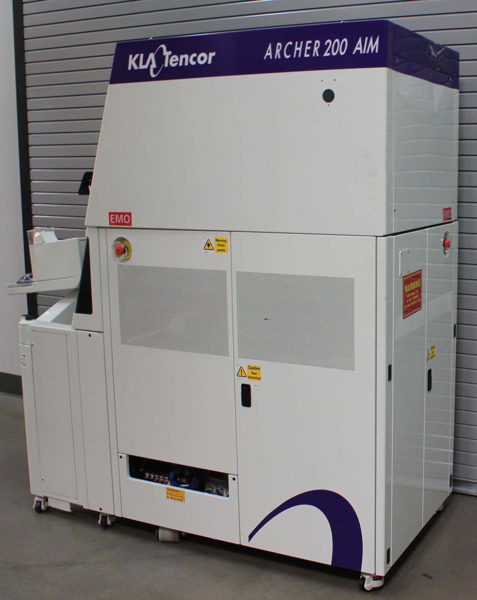

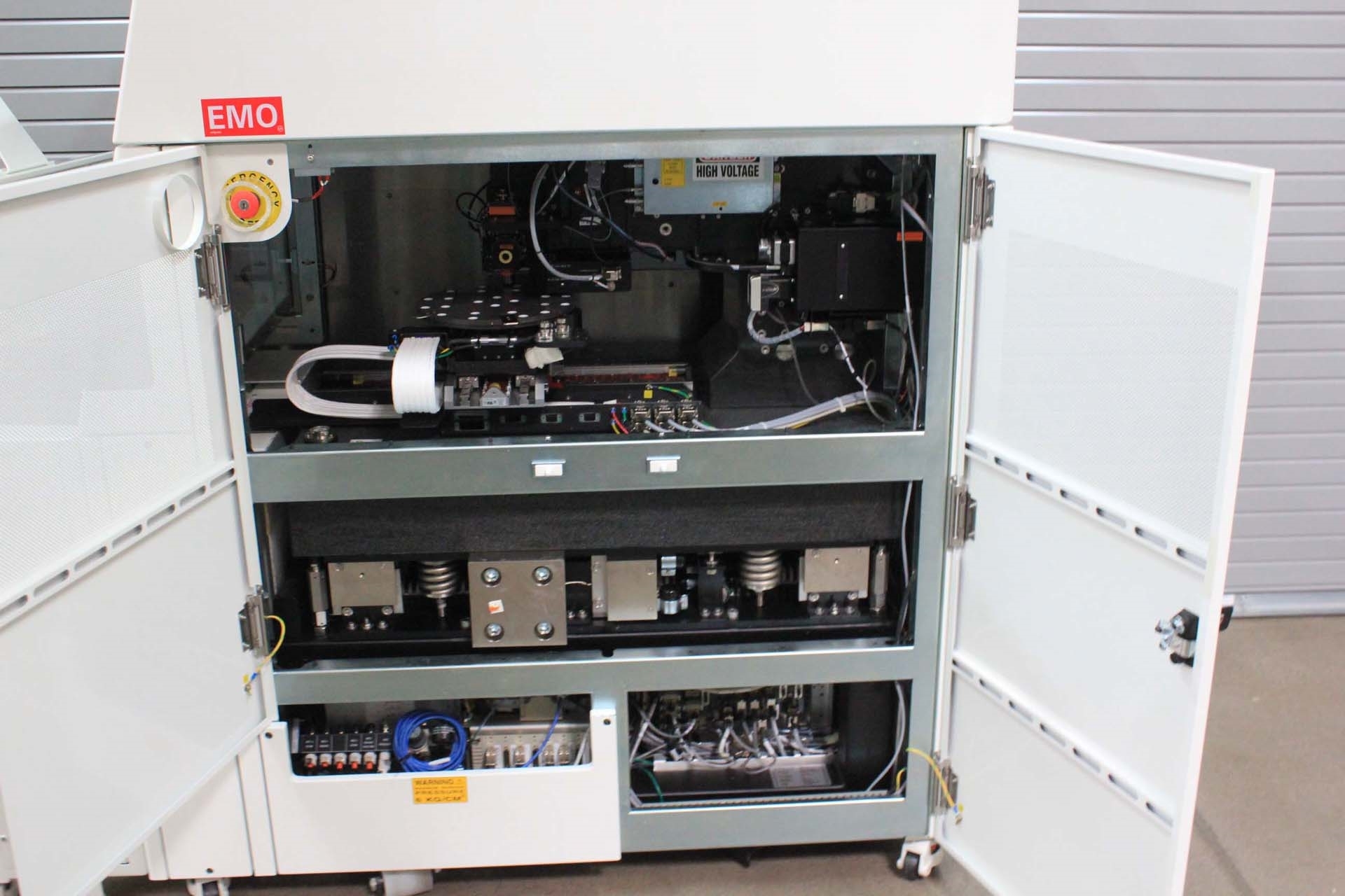

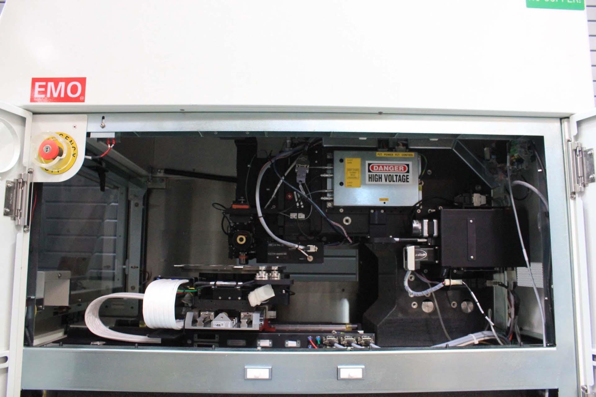

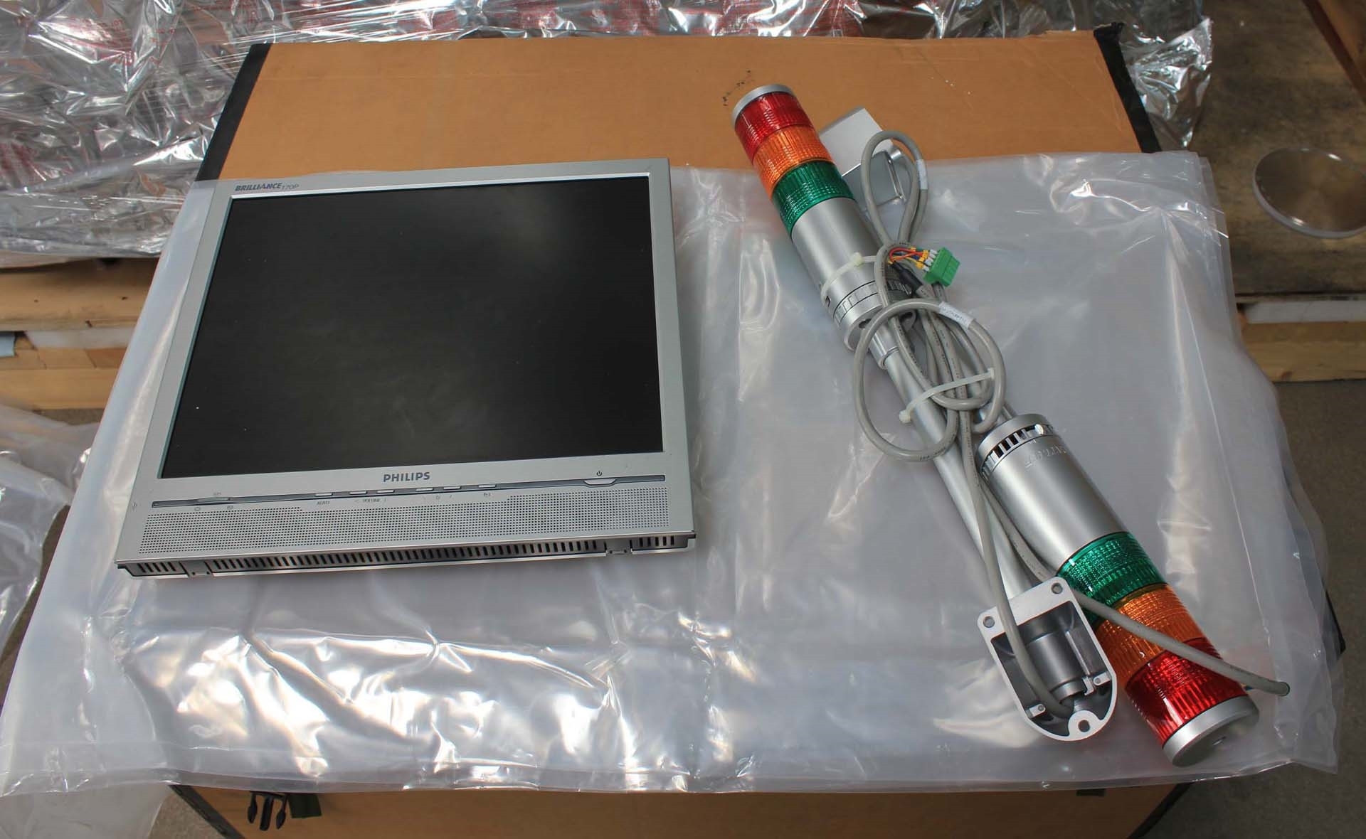

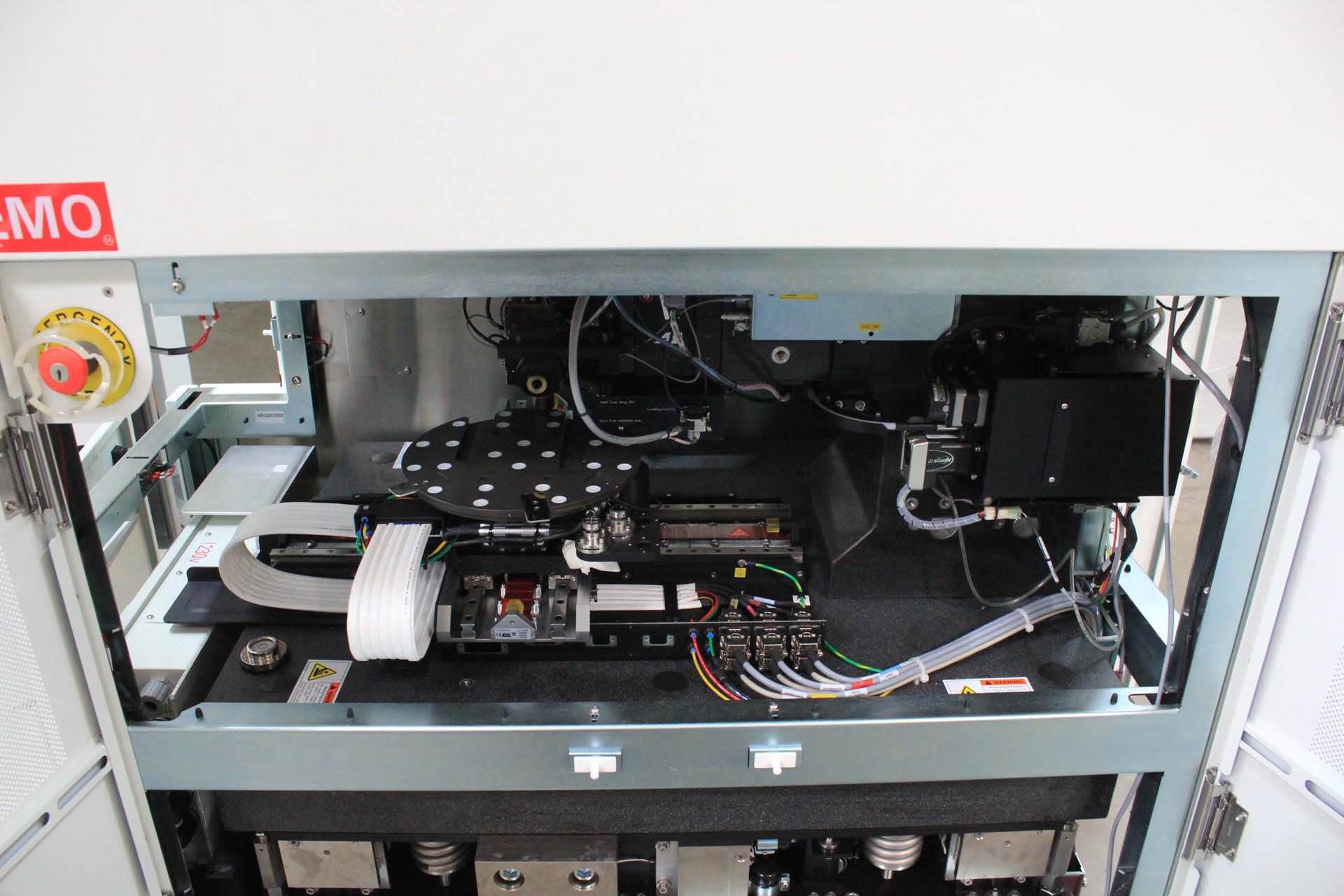


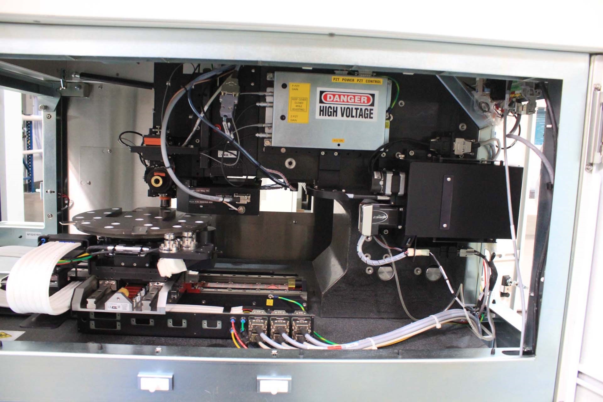

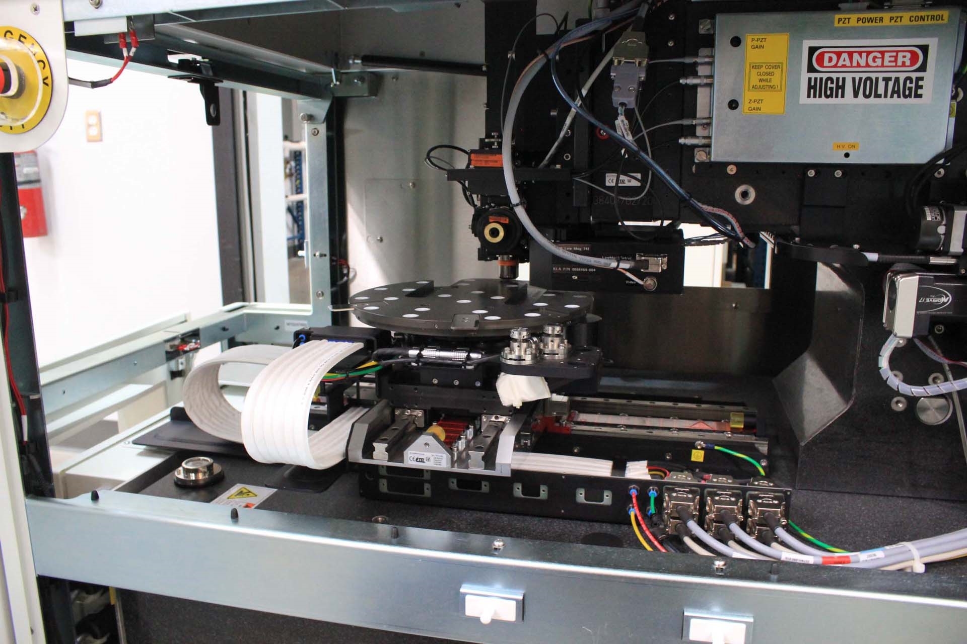

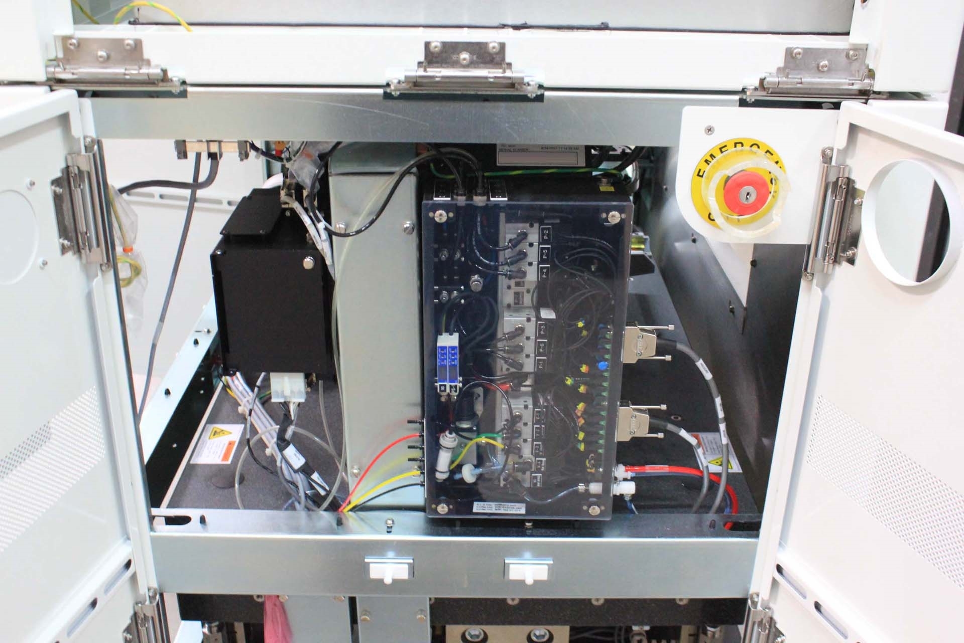

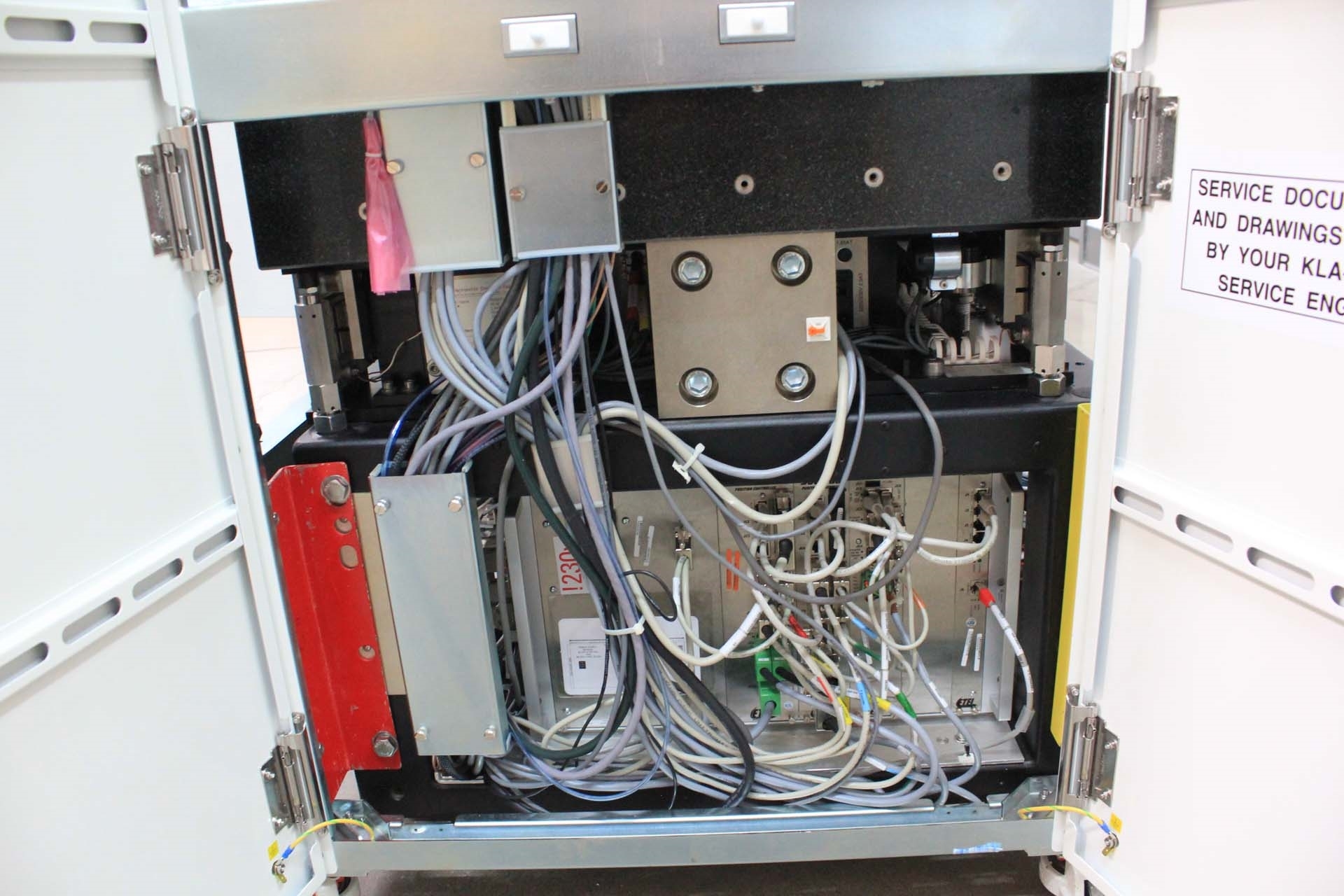

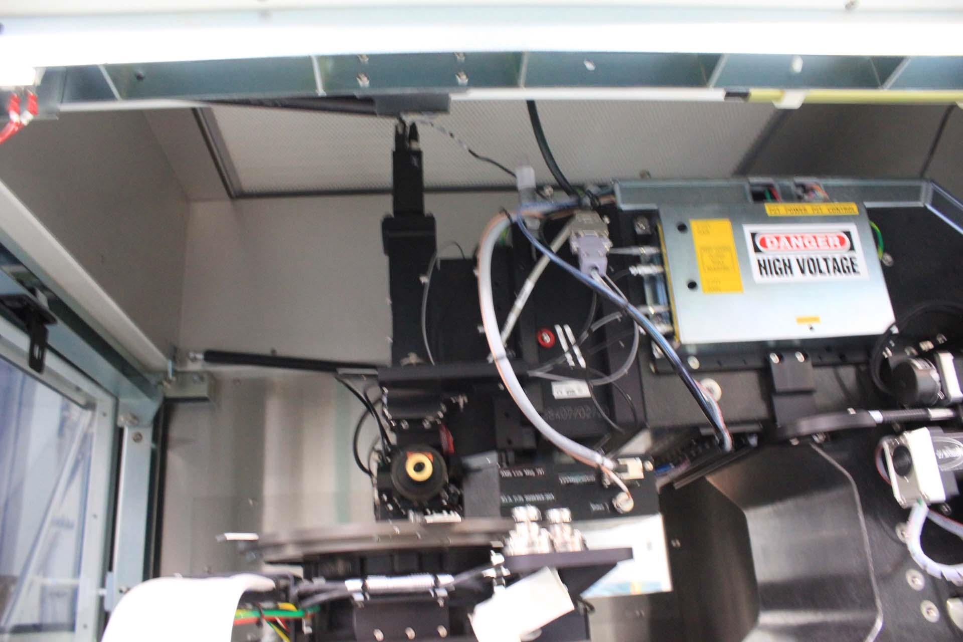

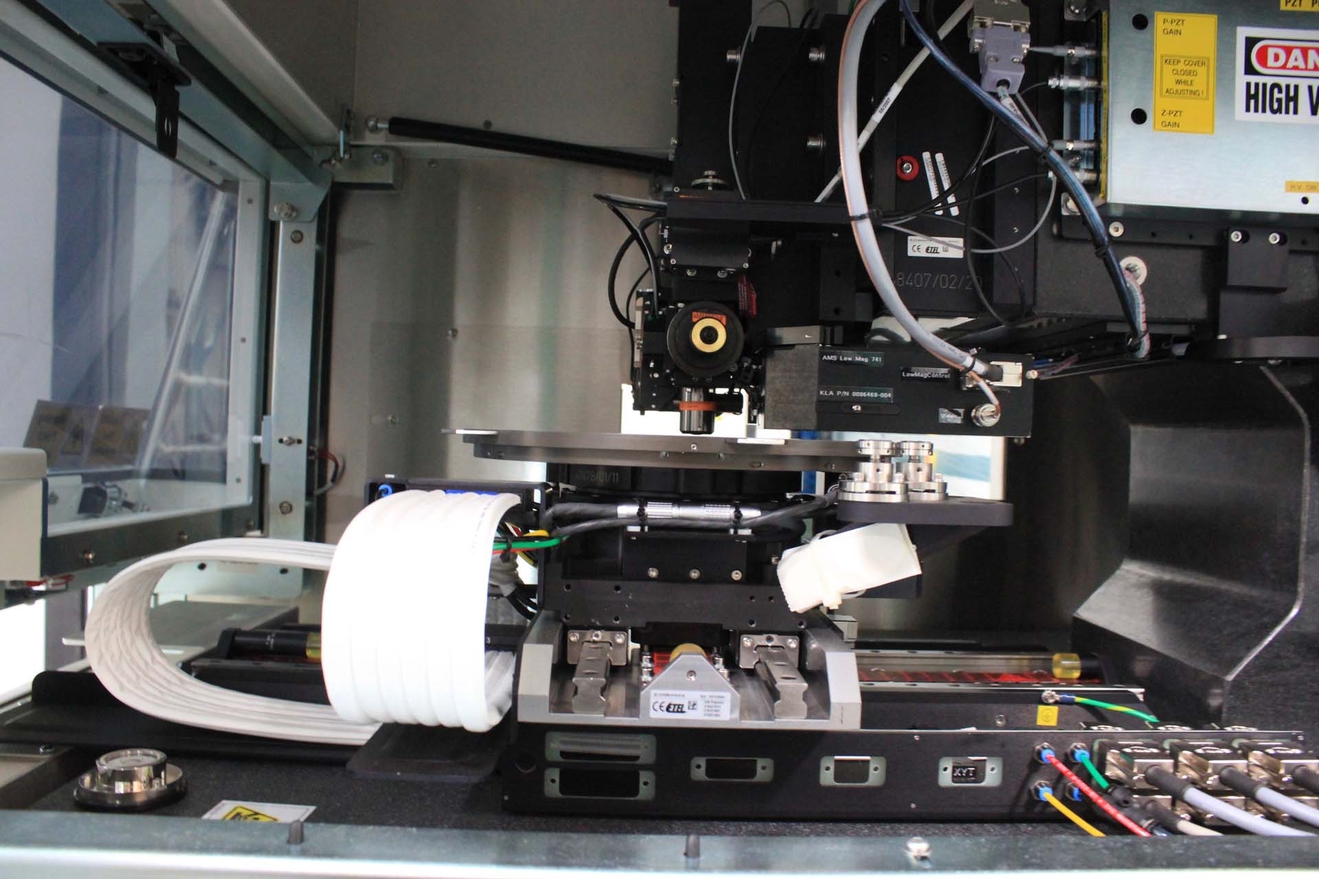


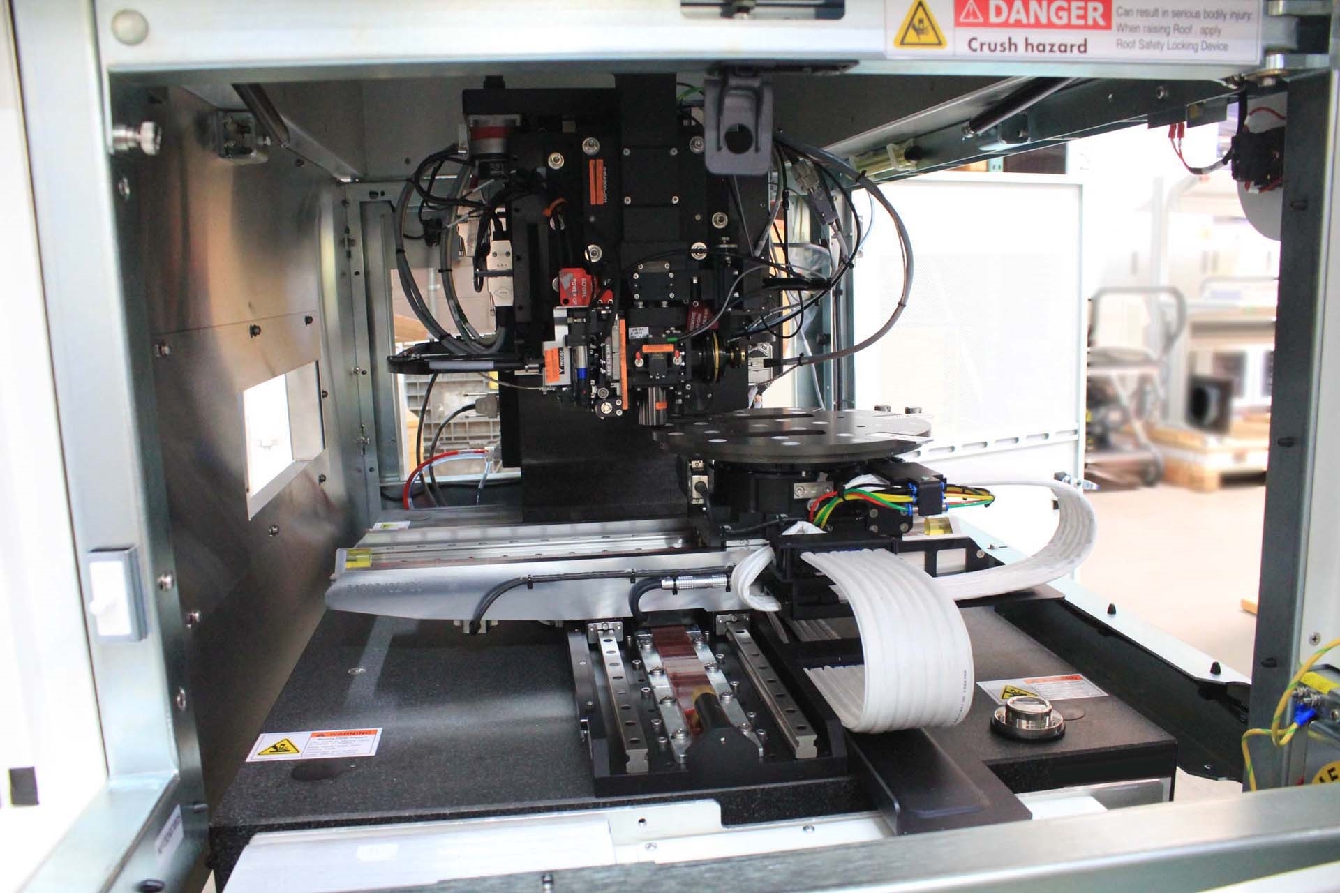

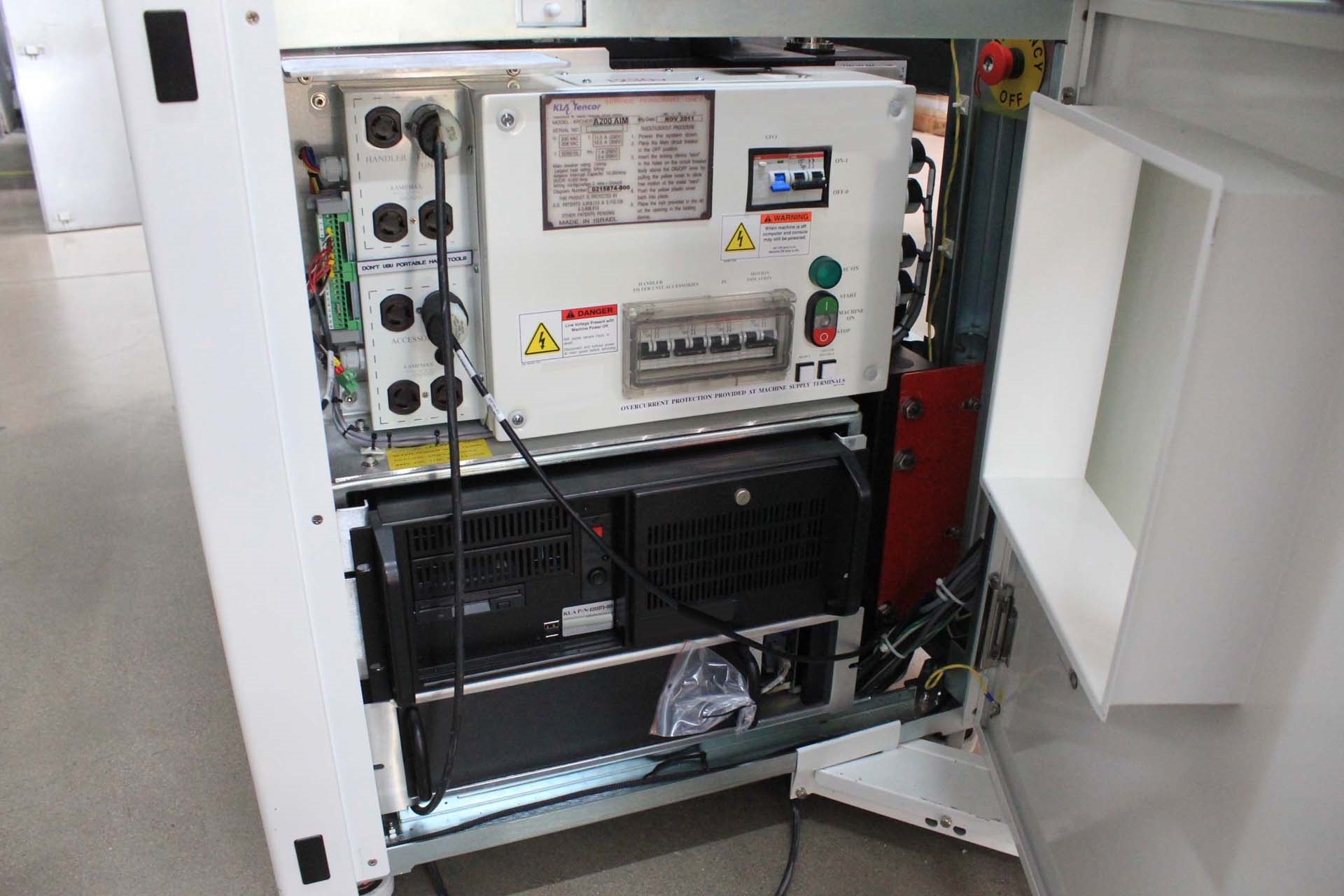

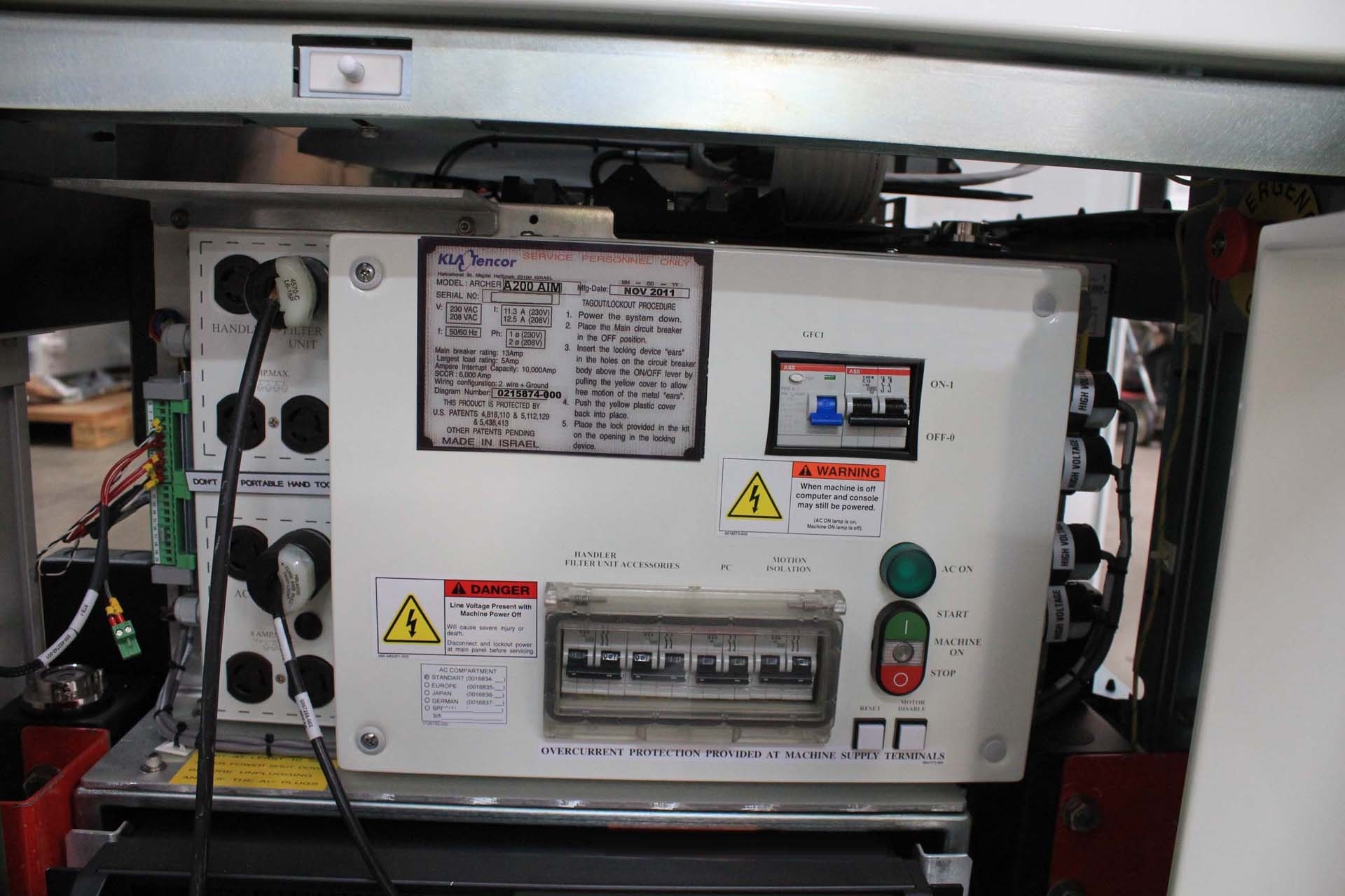



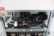
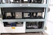
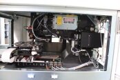
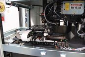
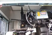
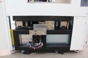
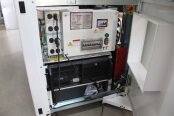
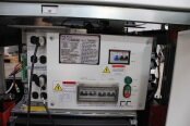
KLA / TENCOR Archer 200 AIM is a mask and wafer inspection equipment for use in the semiconductor industry. It is designed for rapid autofocus, film inspection and die alignment. KLA Archer 200 AIM features high-resolution optics, laser autofocus and light source technology, LED illumination and automated image capture. It also has a small footprint, making it well-suited for automated production environments. TENCOR Archer 200 AIM employs advanced optics and electronics technologies that are optimized for the semiconductor fabrication process. It has multiple video sources for simultaneous inspection of films and die patterning. The illumination system can create uniform light across the entire field of view, providing high contrast imaging accuracy. The optional laser autofocus unit provides excellent results by quickly and accurately focusing on the desired target. The machine also provides automated image capture and storage. It can capture images of films and die patterns in milliseconds and store them in a variety of formats, including TIFF and JPEG. It also supports multiple image filters and image analysis. Archer 200 AIM's advanced imaging capabilities offer excellent performance in inspection of films, wafers and dies. It is designed to detect defects in their various forms, including short circuits, missing parts and wrong materials. It is particularly well-suited for detecting and classifying line edge nonuniformities, as well as for measuring line widths, edge definition and unresolved print features. KLA / TENCOR Archer 200 AIM provides comprehensive die-to-database traceability, enabling it to be fully integrated into a production control tool. Additionally, the asset features an intuitive user interface and multiple levels of model accessibility to facilitate training and maintenance. Overall, KLA Archer 200 AIM is an excellent tool for inspection and analysis of films, wafers and dies. Its advanced optics and imaging technologies enable efficient and accurate analysis and resolution of defects. Its intuitive user interface, multiple levels of equipment accessibility, and die-to-database traceability also make it a great choice for automated semiconductor production environments.
There are no reviews yet

