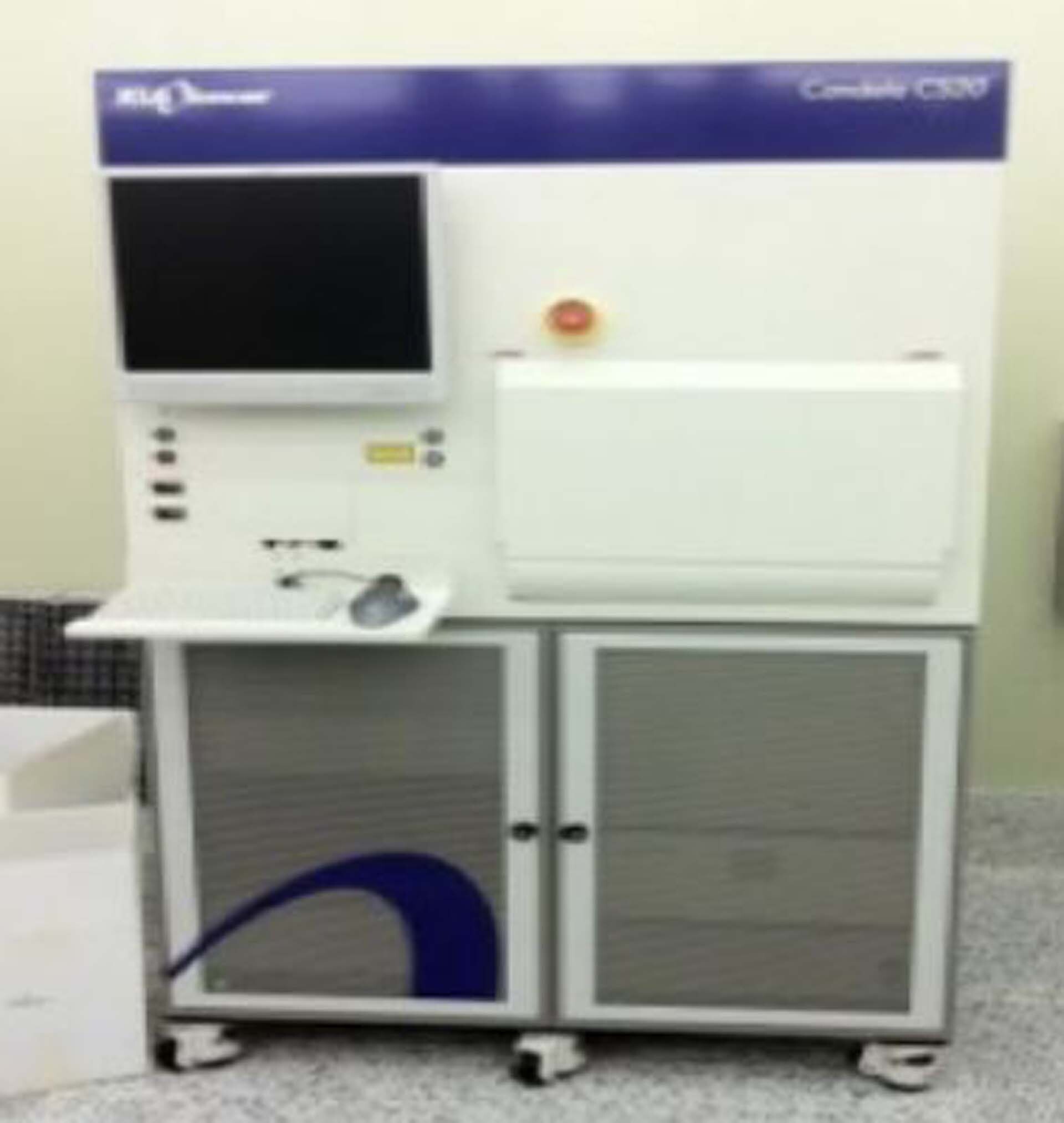
Used KLA / TENCOR Candela CS20 #9390979 for sale
URL successfully copied!
Tap to zoom


ID: 9390979
Wafer Size: 2"- 8"
Particle counter, 2"- 8"
Thickness: 350 µm to 1,350 µm
Defect sensitivity: 0.08 µm Diameter
PSL Sphere equivalent: ≥ 95% Capture rate
Surface topography: >2Å Ra sensitivity
Parameters: Ra, Rq, Wa, Wq
Film thickness uniformity (Single layer): 5Å <Thermal oxide < 1000Å
Depth of focus: Maximum ±15 µm under bow
Repeatability: CV ≤ 5.0 %
Edge exclusion:
Imaging (No exclusion)
Defect analysis, varies with wafer size (Nominal: 2"= 1.5mm, 8"= 5mm)
Defect types:
Particles
Scratches
Stains
Pits
Bumps
Scratches: 100 µm long, 0.1 μm wide, 50Å deep
Pits: 20 µm Diameter, 50Å deep
Stains: 20 µm Diameter, 10Å thick
Illumination source:
50 mW Laser
405 nm Wavelength
R-Θ Coordinates
Coordinate precision: 80th percentile ≤150 µm
Coordinate accuracy: 80th percentile ≤150 µm
Spatial resolution: Minimum ≥ 10m spacing at outer edge of 8"
Single channel particle measurements
Robotic wafer handler, 2"- 8"
Operator interface: Trackball and keyboard
LCD Monitor, 19".
KLA / TENCOR Candela CS20 is a mask and wafer inspection equipment that offers high-speed inspection performance, superior defect detection and analysis capabilities, and high throughput accuracy. The system is capable of detecting defects in semiconductor masks and wafers with precision and accuracy. The unit uses advanced multidimensional defect detection and advanced wafer pattern recognition to rapidly and accurately detect defects in a variety of mask and wafer substrates. The machine is designed to achieve superior wafer recognition rates. It uses a combination of image processing, computer vision, pattern recognition and multidimensional defect detection algorithms to accurately identify and analyze imperfections. The tool uses two camera head stages and advanced optics to capture and analyze the pattern on the mask or wafer at the same time. This provides a double pass for detection and analysis, enabling faster scanning times and superior accuracy. The asset also features 360-degree angle inspection, which allows users to rotate the wafer or mask in any orientation without losing its accuracy and providing full coverage for defects. It also includes multiple automated alignment, sensitivity and edge focus adjustment options for precision imaging. The model also includes advanced probing capabilities for characterizing marker edge placement, CD and CDU accuracy, particle counts and more. The equipment features a wide variety of user options and features. It has a built-in color display which offers quick navigation and intuitive control of the mask or wafer inspect process. It also contains a Windows XP-based software package which offers enhanced graphical setup and control. In addition, the system is equipped with a powerful analysis engine which performs powerful 2D pattern analysis. The unit also offers network connectivity and can be connected to many other inspection and analysis programs. This allows users to connect to other parts of the inspection machine when needed, provide remote control of the tool, as well as synchronize and store data. This enables users to maximize the speed and accuracy of the inspection asset. KLA CANDELA CS-20 mask and wafer inspection model is an ideal choice for precision semiconductor manufacturing due to its superior performance, accuracy, and speed. The advanced features and technologies included with the equipment provide users with an intuitive, quick, and reliable scanning solution for the inspection and analysis of semiconductor masks and wafers.
There are no reviews yet