Used KLA / TENCOR eDR-5210 #293755072 for sale
URL successfully copied!
Tap to zoom
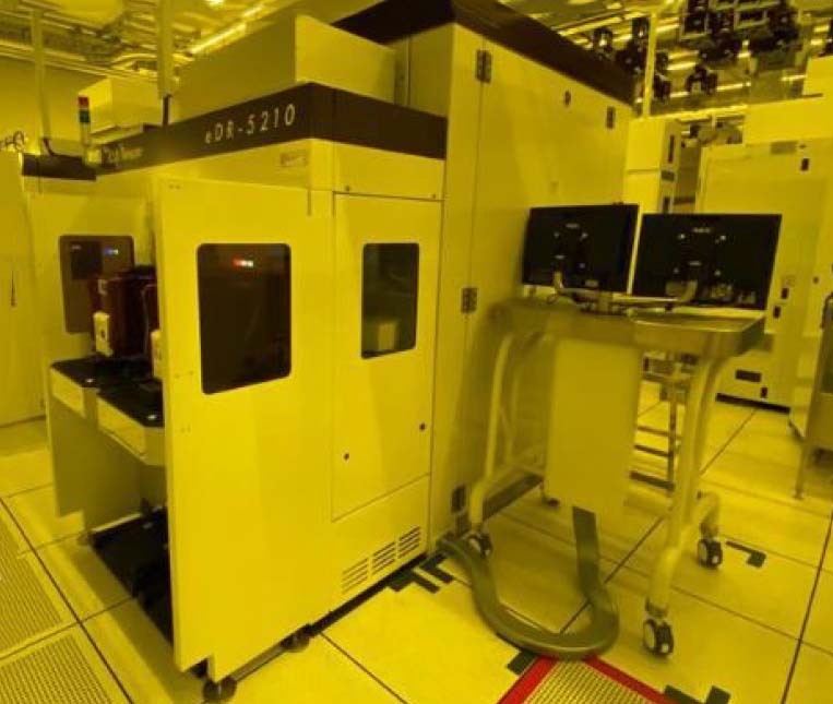

ID: 293755072
Wafer Size: 12"
Vintage: 2010
Scanning Electron Microscope (SEM), 12"
2010 vintage.
KLA / TENCOR eDR-5210 is an automated mask and wafer inspection equipment designed to detect defects on the surface of semiconductor materials. It is an application-specific system designed to quickly scan and detect defects on a wafer's surface, providing consistent, repeatable, and reliable results. The unit offers superior performance and utilizes a powerful suite of inspection algorithms to detect a wide range of potential defects, including reflectivity, shift, voids, malformed chip edges, and scratches. The machine uses a 12" projection optics tool to provide ultrasharp delineation of features down to 4 microns and a range of contrast levels dependent on the nature of the material being inspected. Light sources include a green LED (550 nm) and a blue LED (450 nm) for operational flexibility. The aim of the asset is to identify any foreign matter and evaluate potential defects on the wafer's surface. KLA eDR-5210 also features a high-speed, multi-axis motion model with a linear travel speed of 20 m/s. The automated alignment optics minimize back-scattered and stray light, allowing it to move accurately and quickly over the entire surface to detect even the slightest of defects. It can quickly scan the entire wafer surface from top to bottom and can even detect positive-negative polarity defects, a feature that can help to reduce post-processing time. The equipment is also capable of optimizing a wide range of imaging techniques, including high-resolution edge detection, contrast enhancement, and defect detection. Through its sophisticated imaging technologies, TENCOR EDR 5210 is able to provide accurate information for improved decision-making and utilization of resources. Additionally, its fully automated operation reduces the labour costs associated with manual inspection. Overall, TENCOR eDR-5210 is an automated, application-specific system that provides significant advantages for manufacturers in the semiconductor industry by providing higher throughputs, comprehensive defect coverage, and consistently reliable results. Its powerful suite of inspection algorithms and range of imaging techniques ensure the highest level of accuracy and performance.
There are no reviews yet