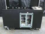
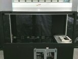
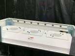
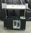
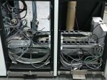
Used KLA / TENCOR EFEM #9276751 for sale
URL successfully copied!
Tap to zoom
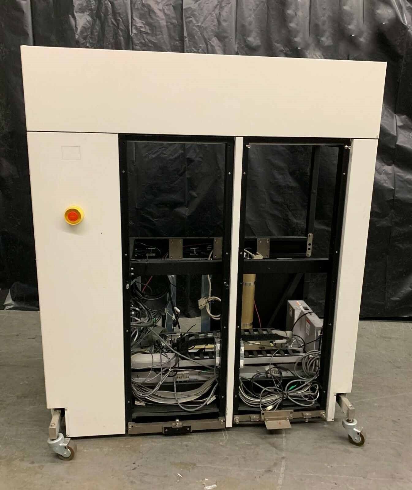

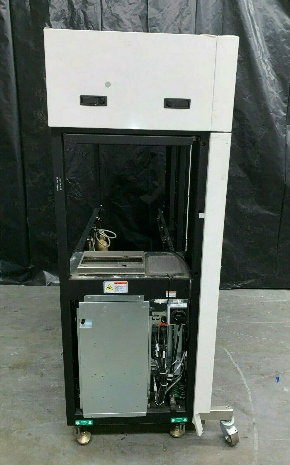


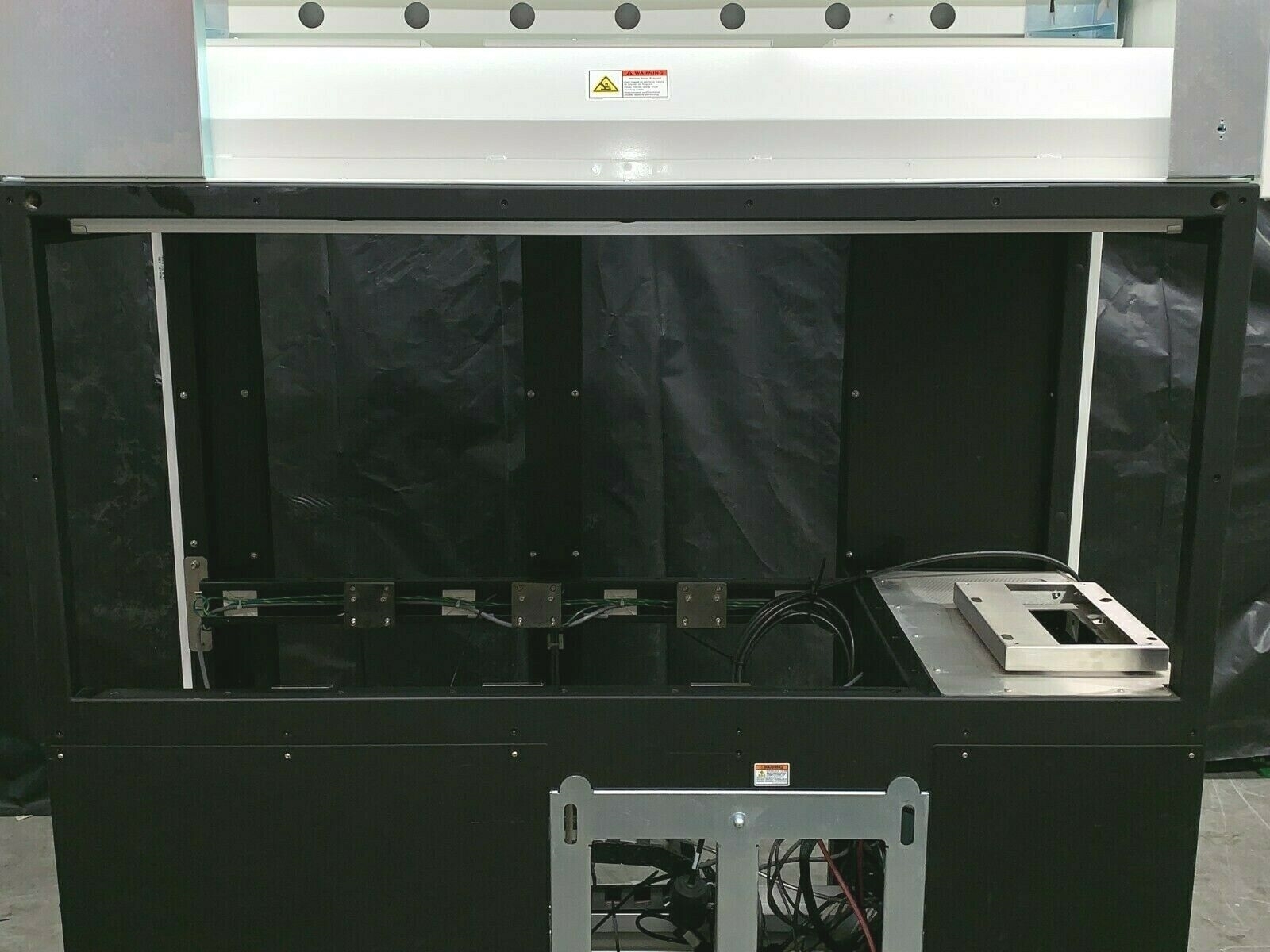

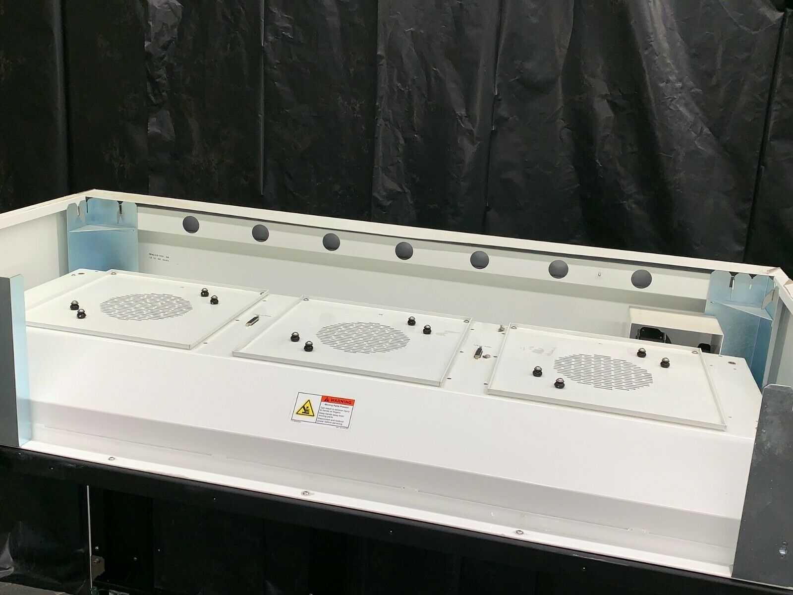


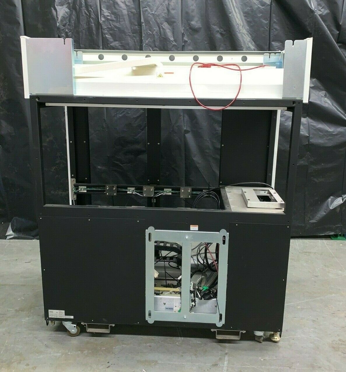






ID: 9276751
System
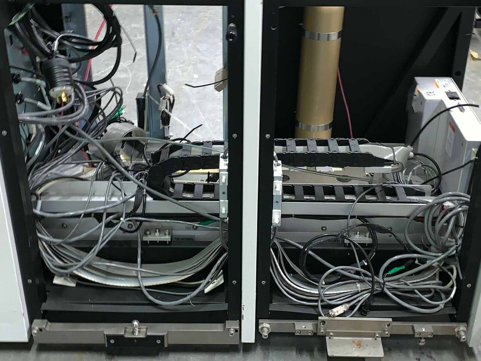
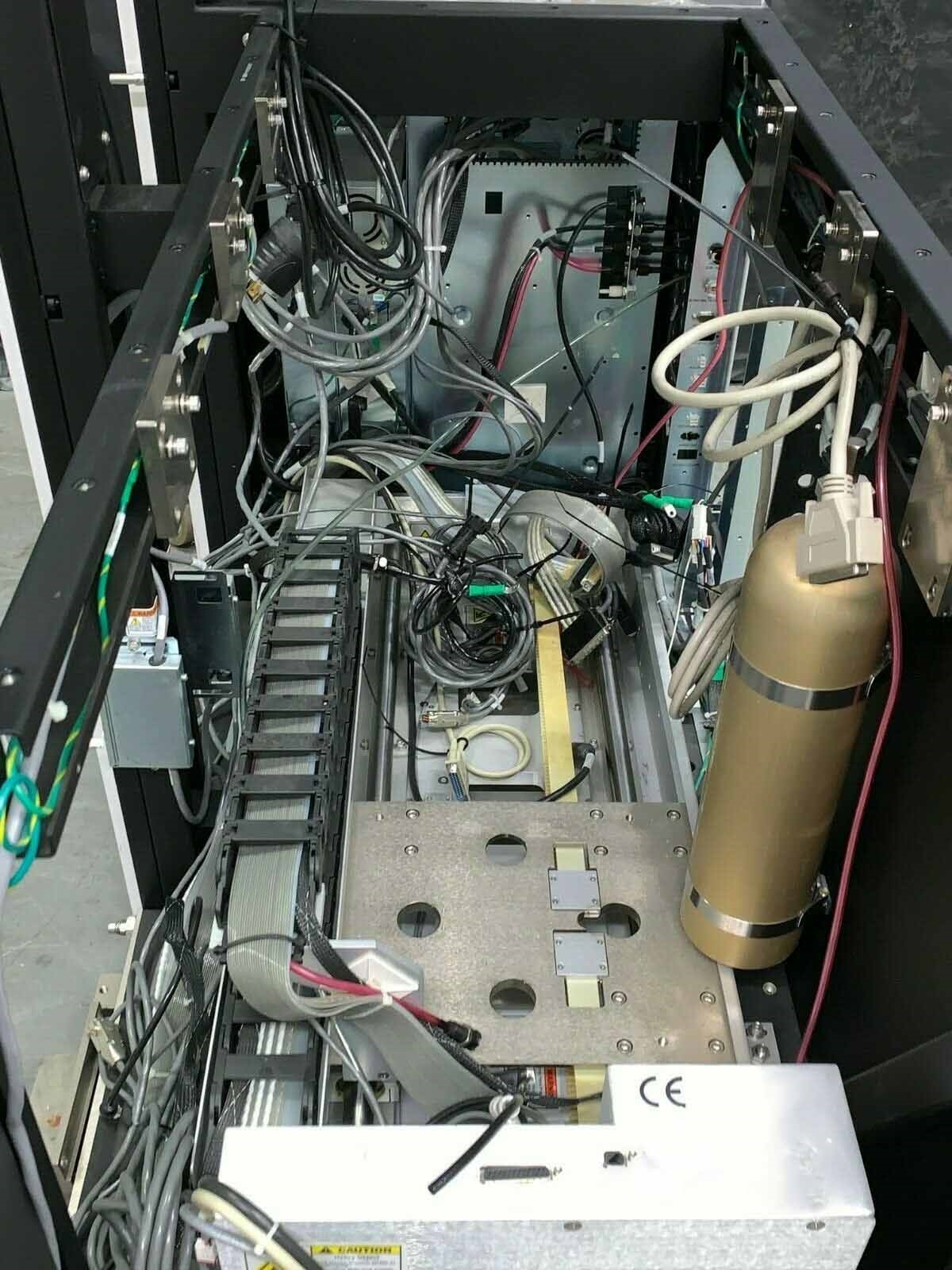
Factory interface
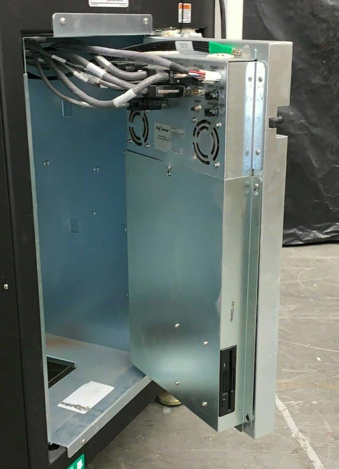
Interface computer
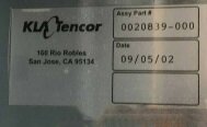
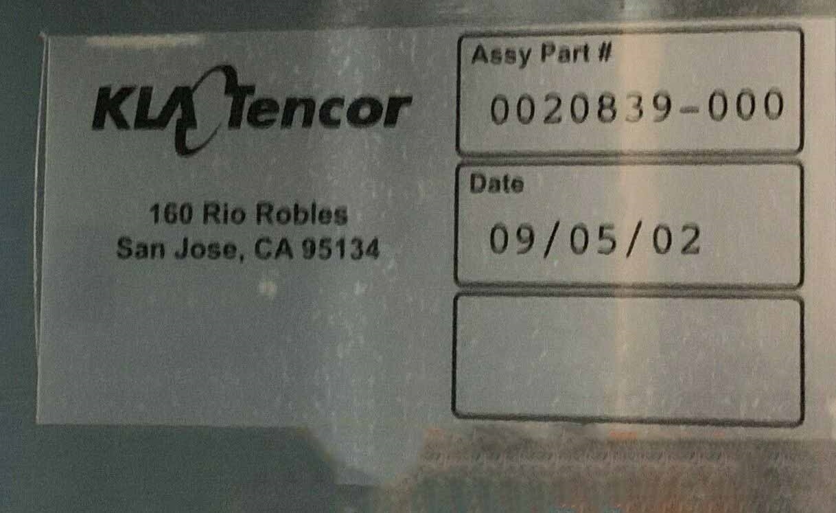
Part number: 0020839-000
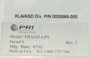
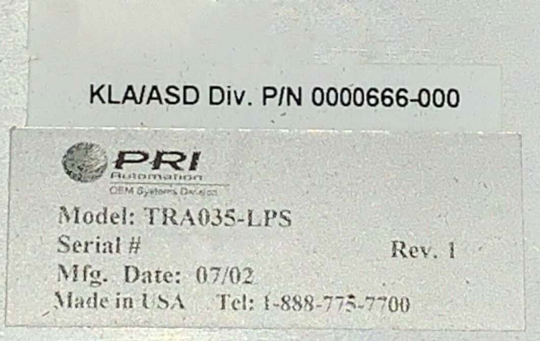
PRI / BROOKS TRA035-PLS Robot Rail
Part number: 0000666-000.
KLA / TENCOR EFEM (Edge and Film Emission Metrology equipment) is an advanced mask and wafer inspection solution designed to accurately detect defects in semiconductor processes. The system uses advanced high-resolution imaging techniques to create profiles of the etched surface of the device and to measure the composition of the resulting film stack. This provides high-precision and granular measurements of within-die variations of the transferred photomask features and photosensitive material and features present on a wafer. KLA EFEM unit combines the efficiency of an automated machine with the accuracy of a human operator. It is engineered to detect micro-defects as small as 20nm, with a typically detection rate of 98%. The tool is available in both differentiating and non-differentiating configurations. The differentiating configuration allows operators to rapidly identify within-die variation, and the non-differentiating configuration allows for more accurate characterization of large-scale features throughout the wafer surface. The asset is composed of hardware, software, and accessories that provides comprehensive process control. It includes global edge emission (GEM) reflectometry and film emission (FEM) reflectometry, both of which employ advanced imaging and analysis. The model also includes low kV imaging; patterned interface (PI); multi-spectral imaging (MSI); edge/film metrology (EDFEM); patterned conductor metrology (PCM); and parametric control (PA); all of which offer comprehensive solutions for accurately measuring the physical characteristics of the substrates. In addition to visual inspection, TENCOR EFEM equipment can also provide a wide range of process control features. It includes a set of embedded sensors that support process-control setups, allowing for high-accuracy identification of non-uniformities in process uniformity (PU) as well as other process variations. The system also provides complete pattern matching capabilities, which enable users to identify and exploit non-uniformities by adjusting pattern matching parameters. EFEM is designed for scalability and can be adapted to the needs of manufacturers regardless of their size and complexity. Its versatile design enables a high degree of customization and provides comprehensive process-control, which significantly reduces costs associated with mask fabrication. With its advanced imaging capabilities and process-control features, the unit is an essential partner for any semiconductor manufacturer.
There are no reviews yet


