Used KLA / TENCOR es20xp #9253037 for sale
URL successfully copied!
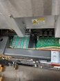
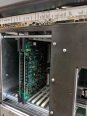
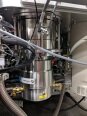
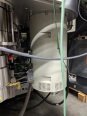
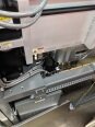
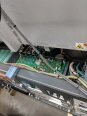
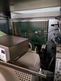
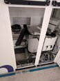

Tap to zoom
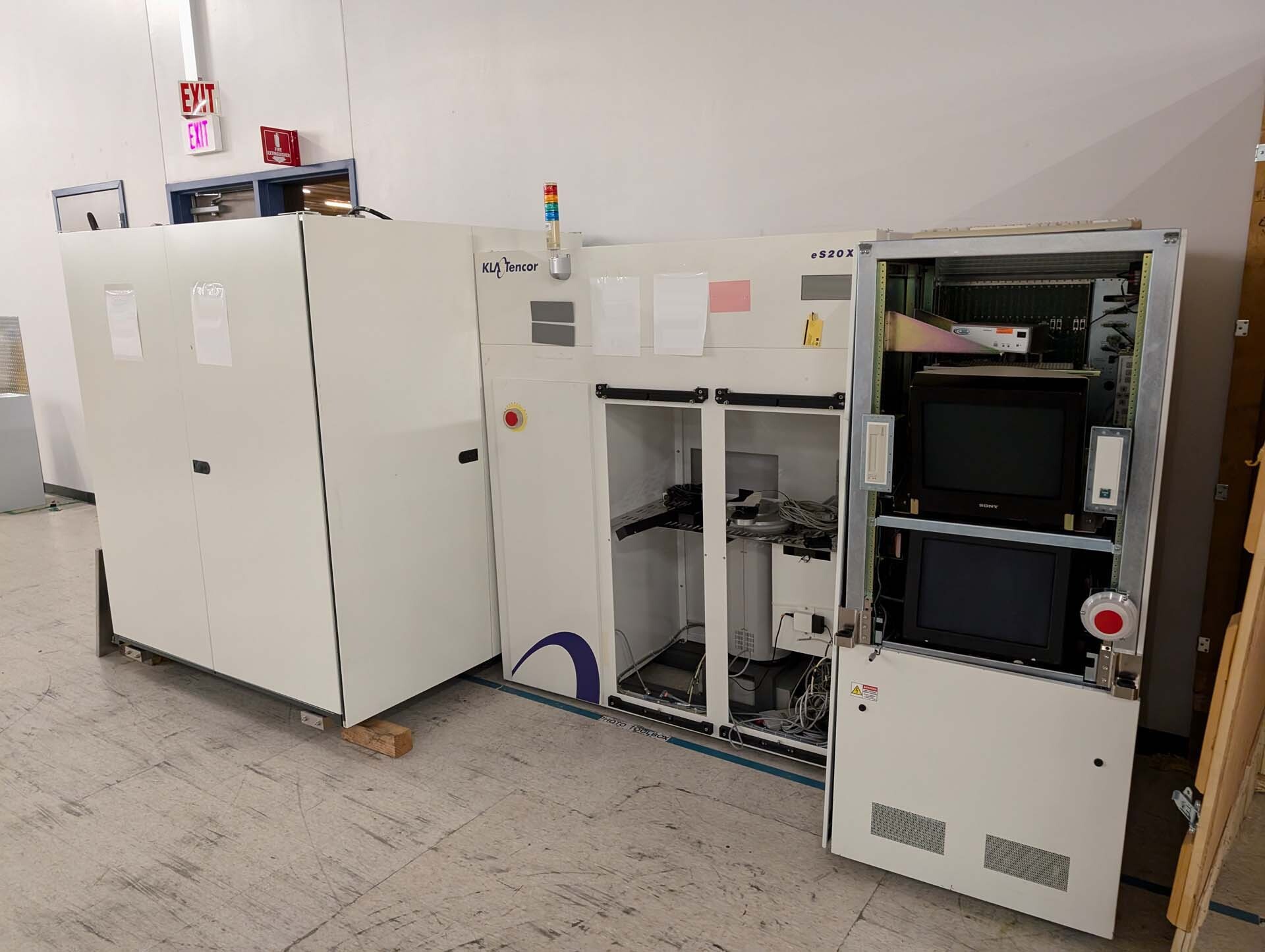

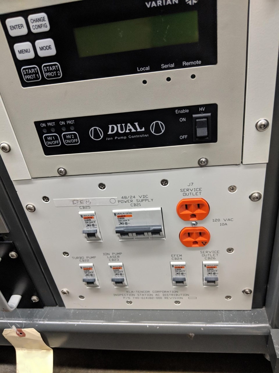
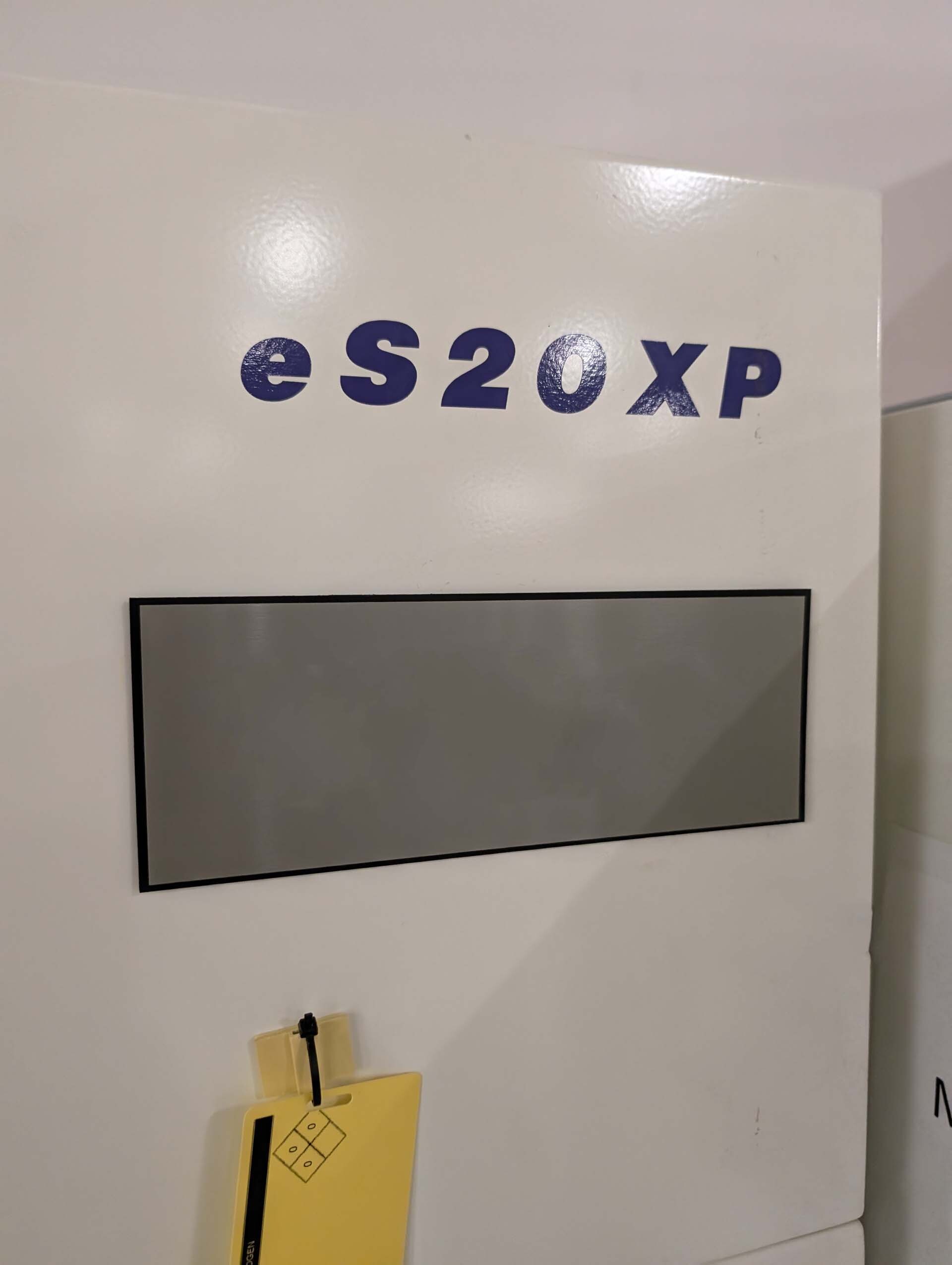
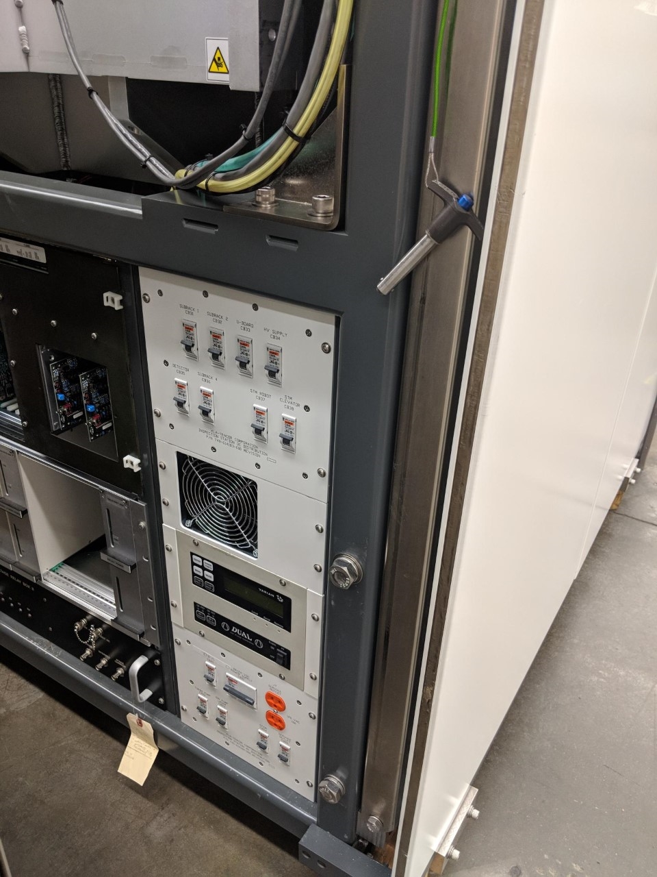
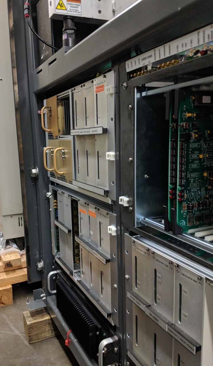
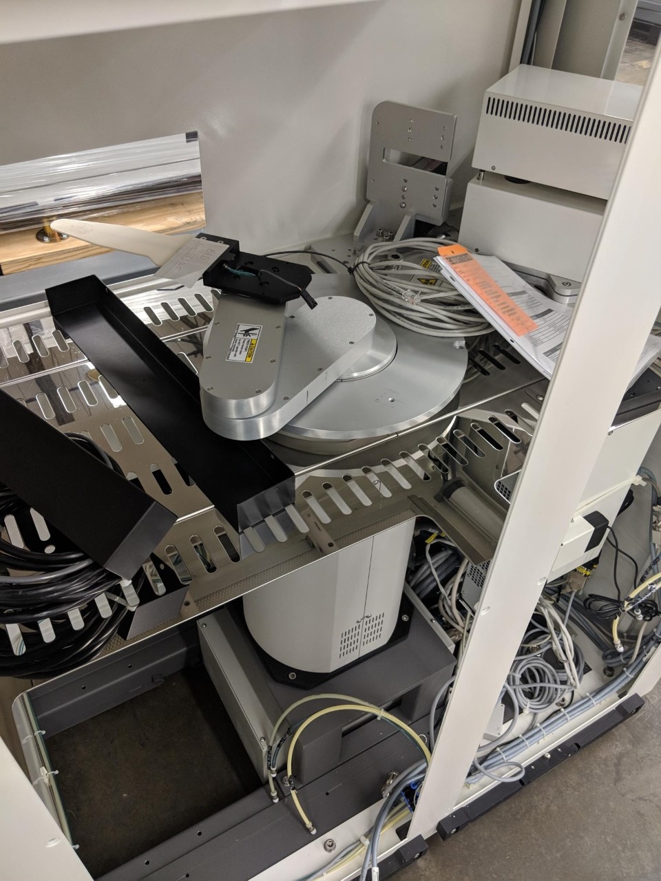
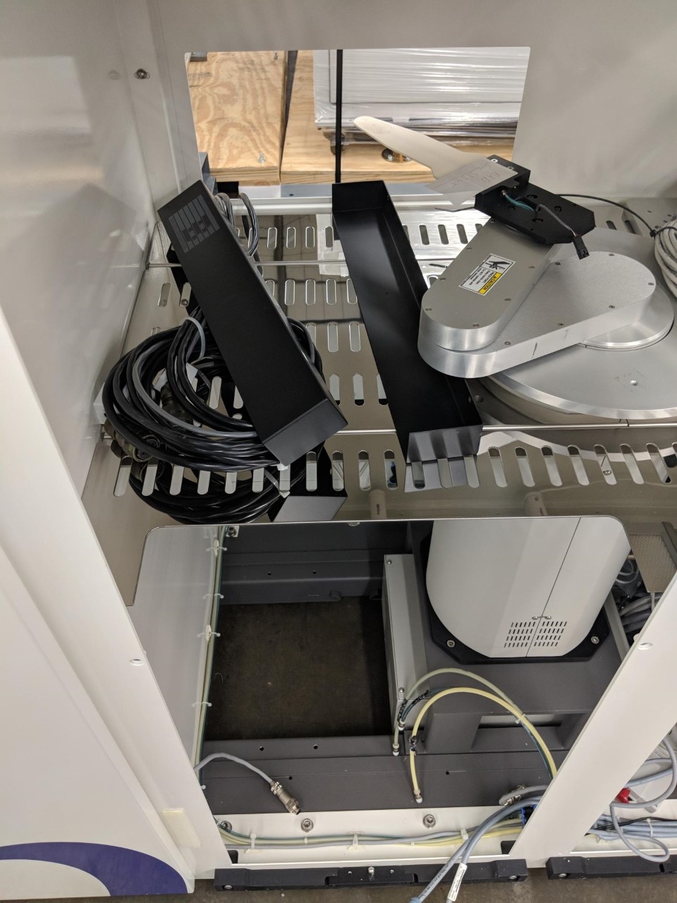
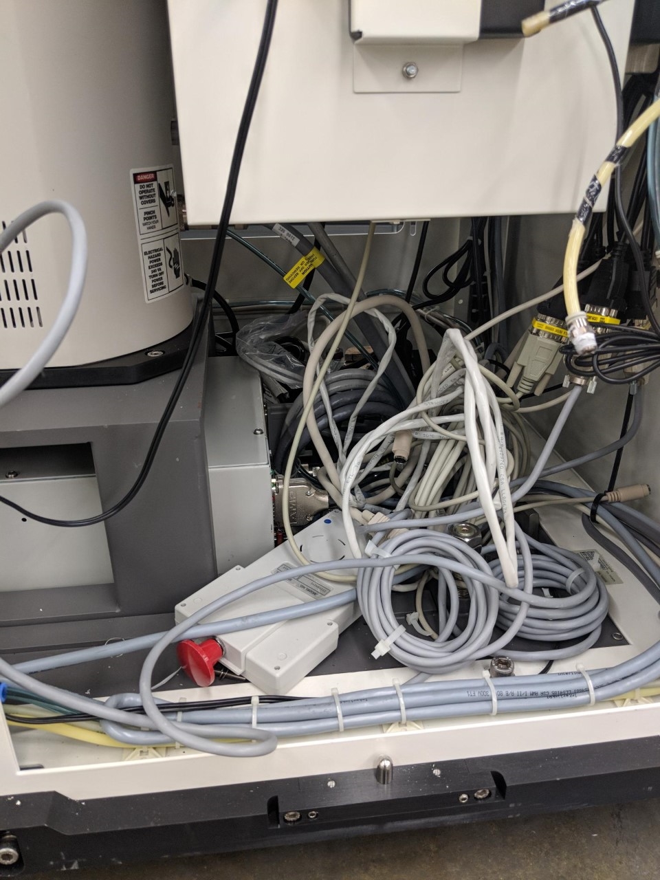
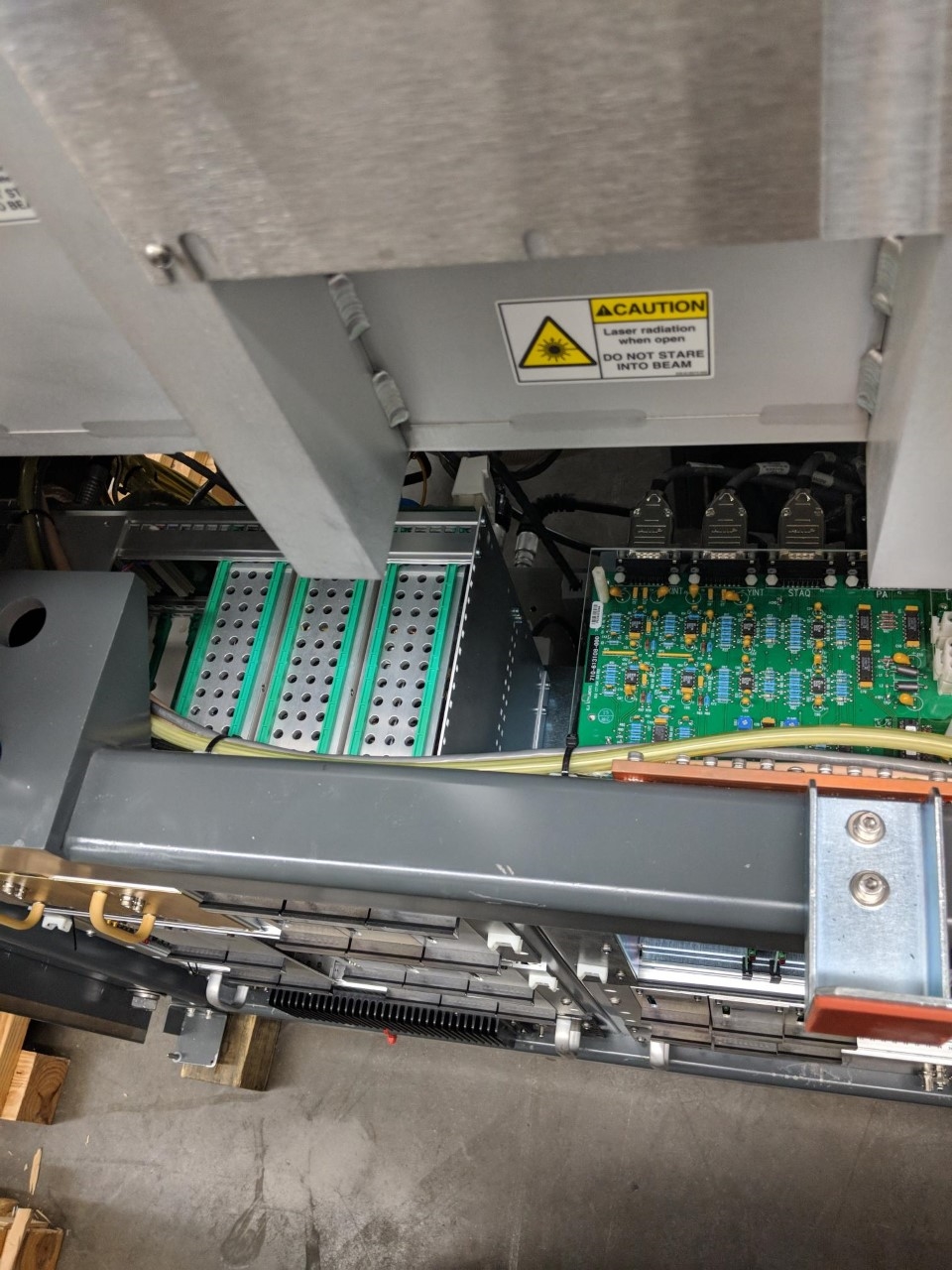
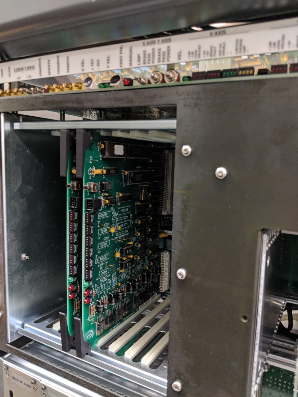
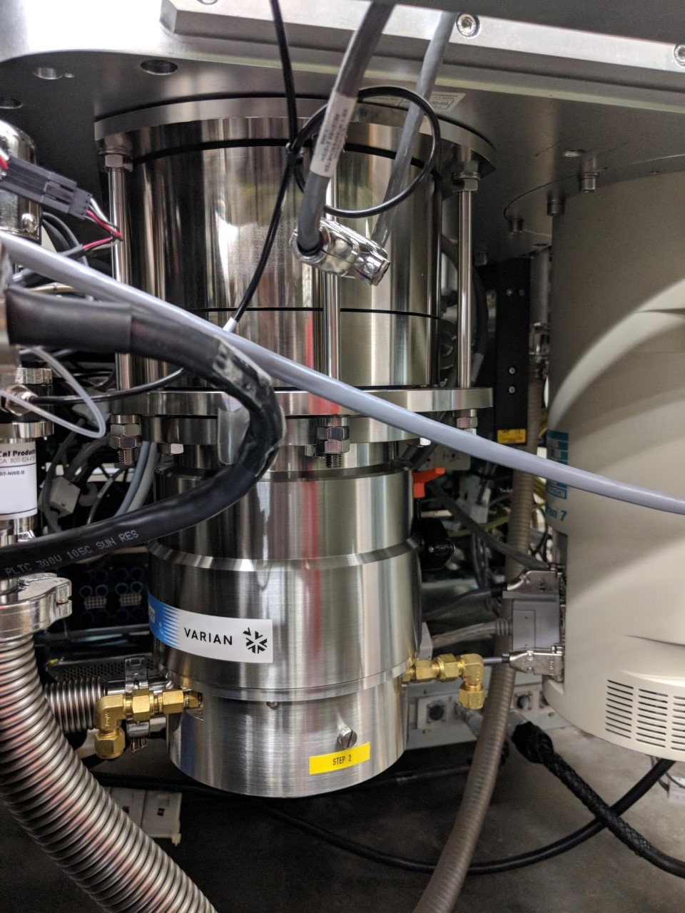
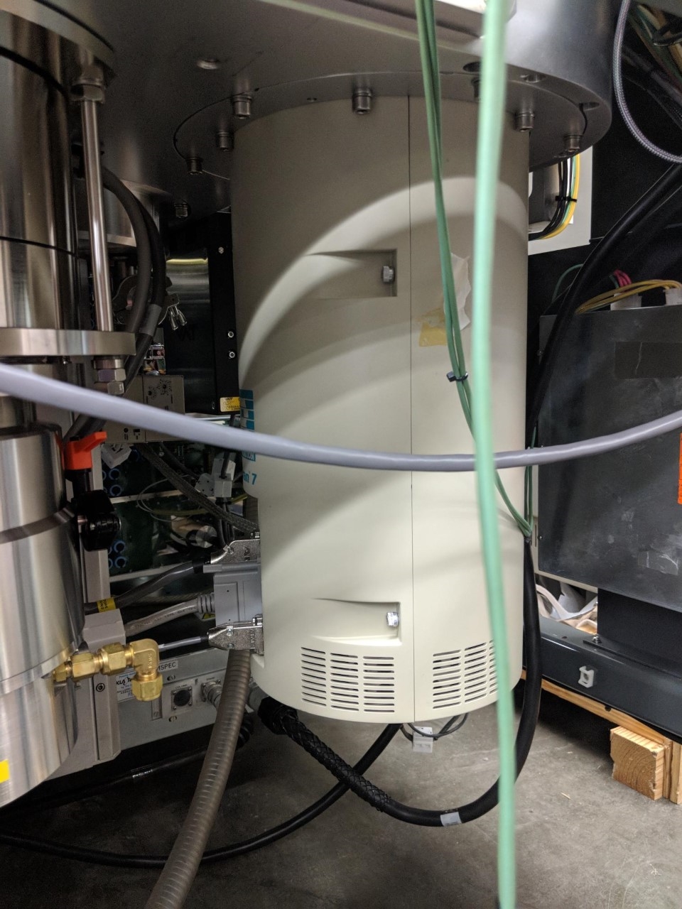
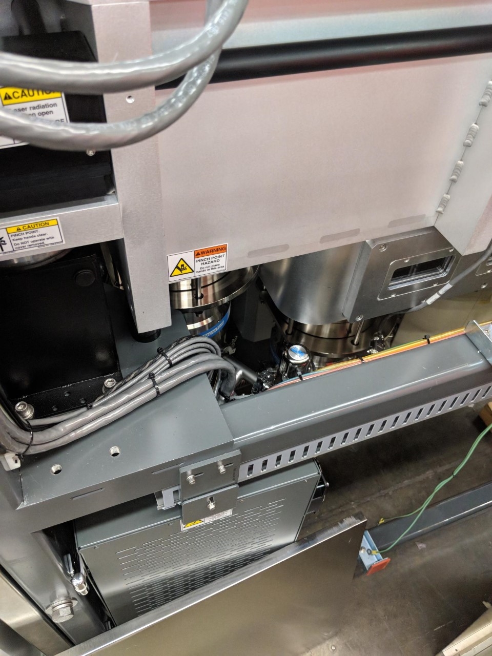
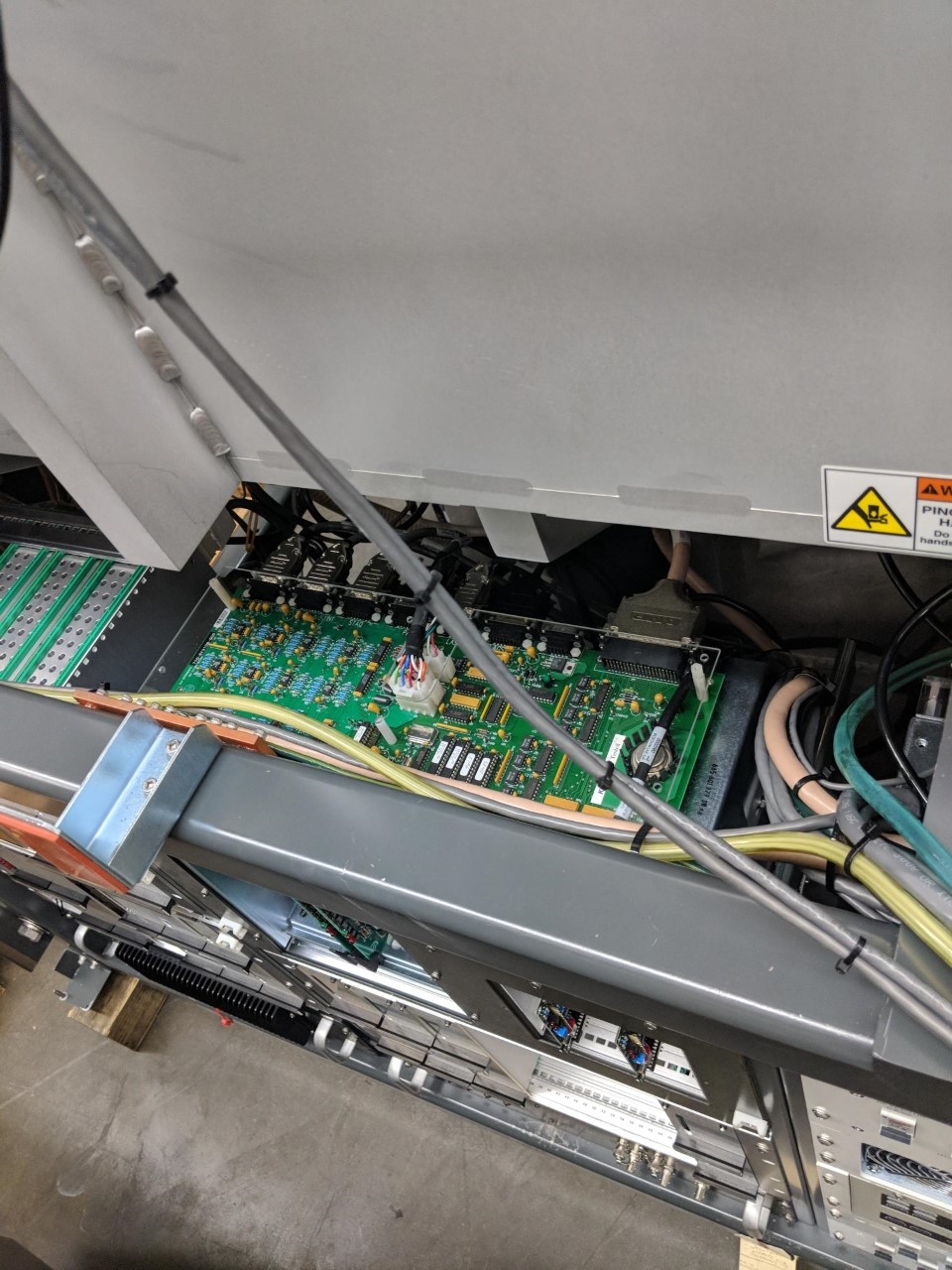
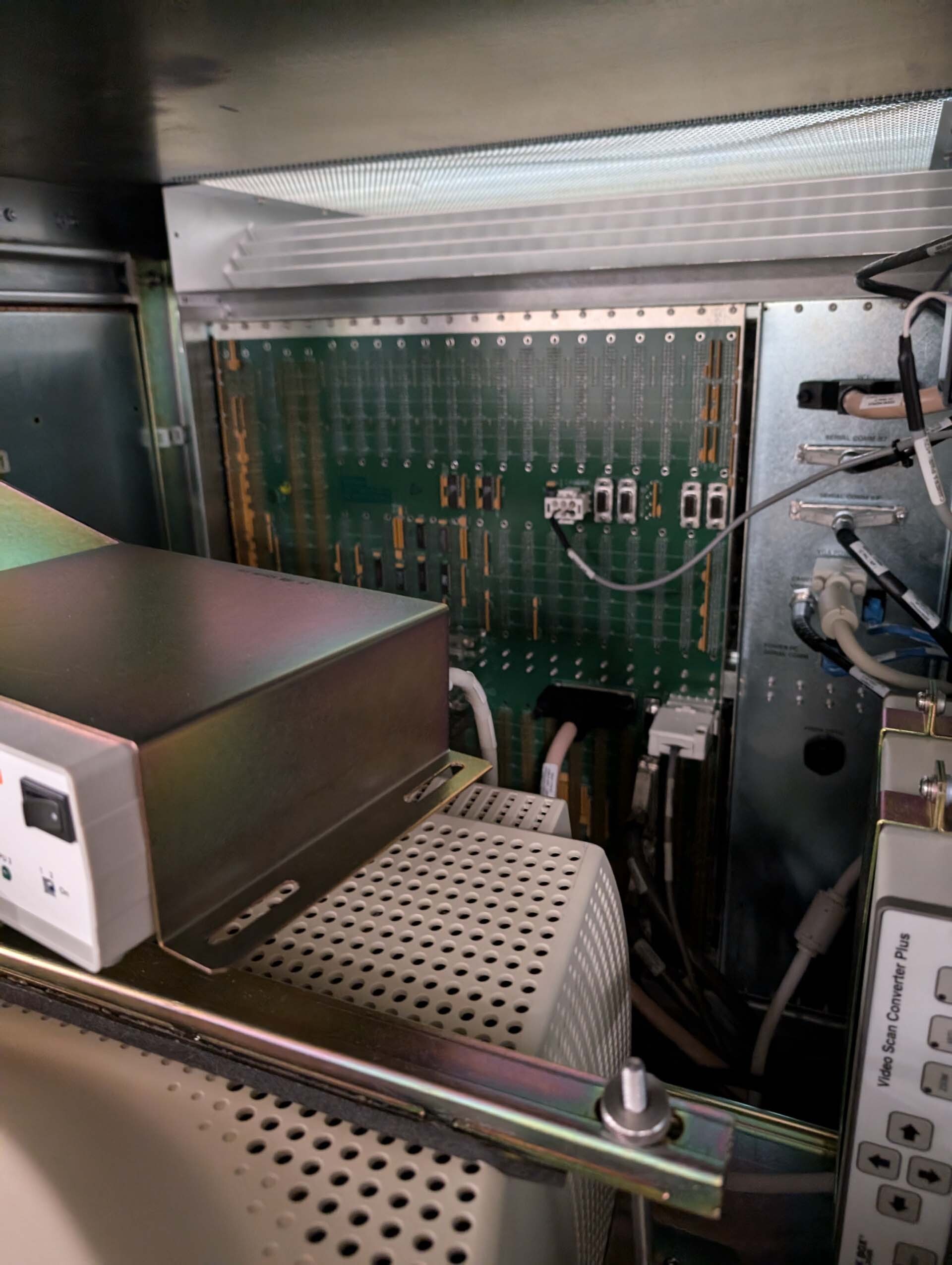
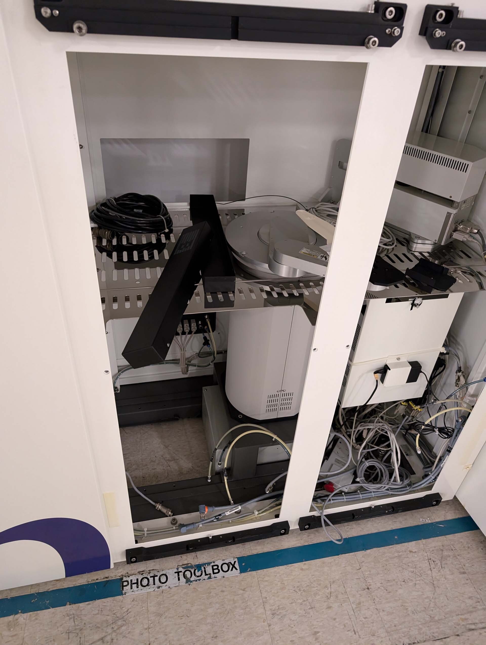
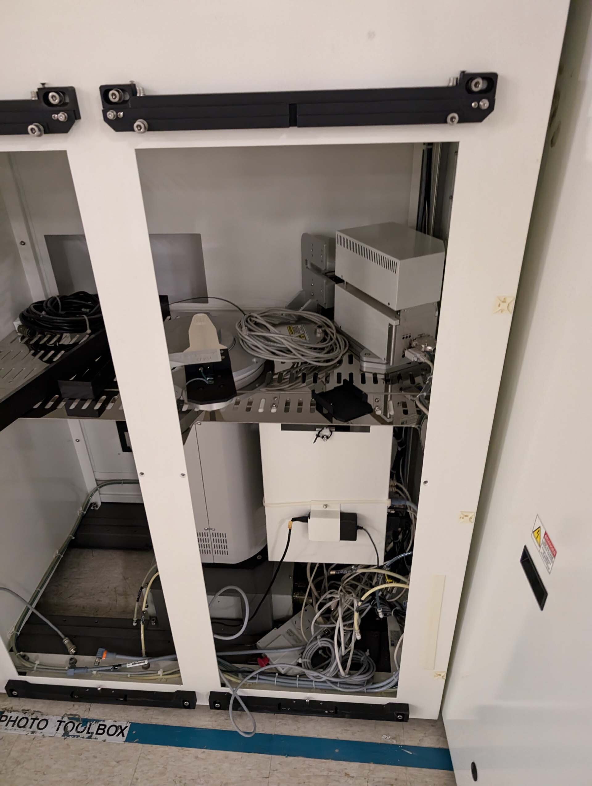
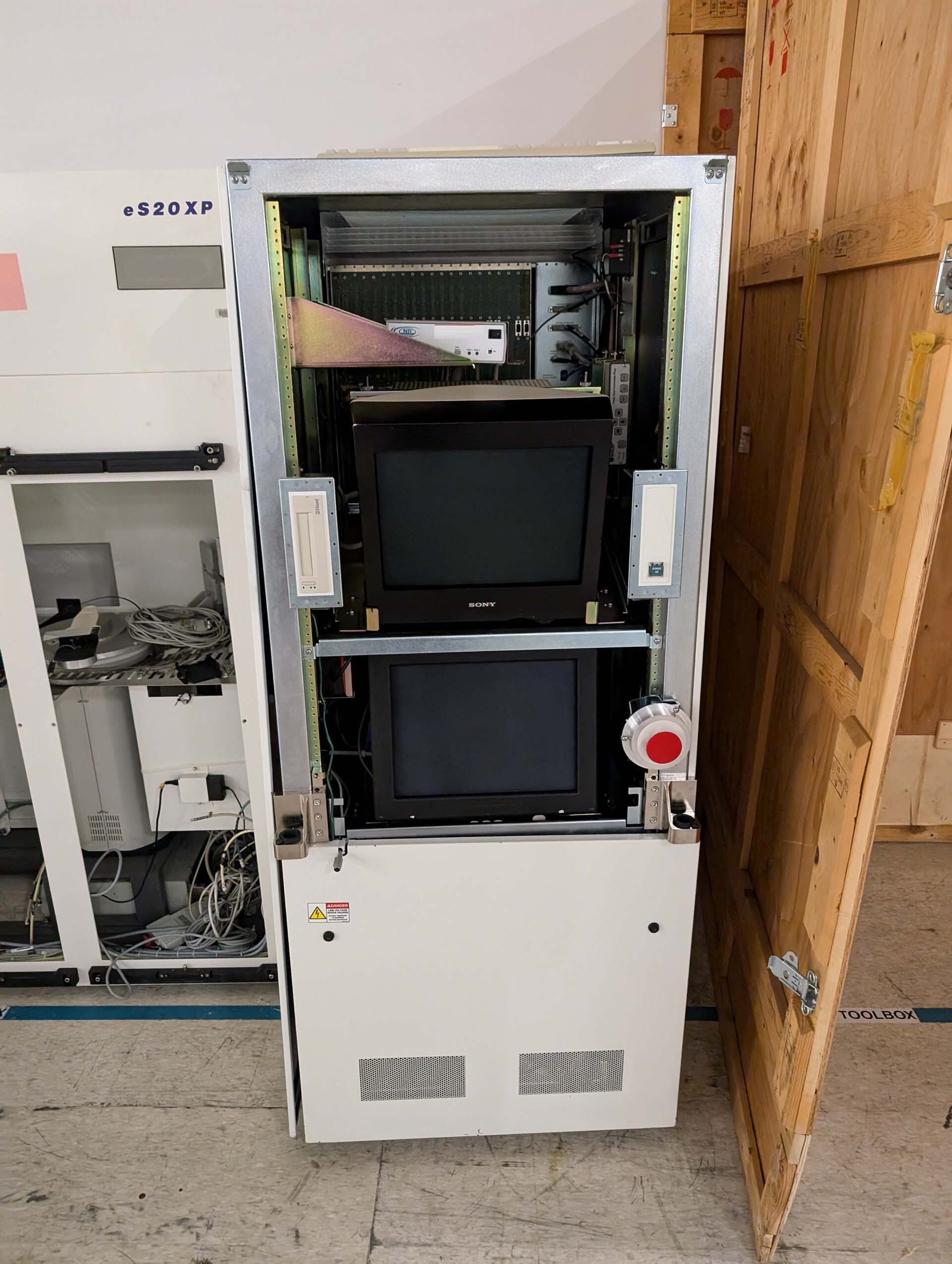
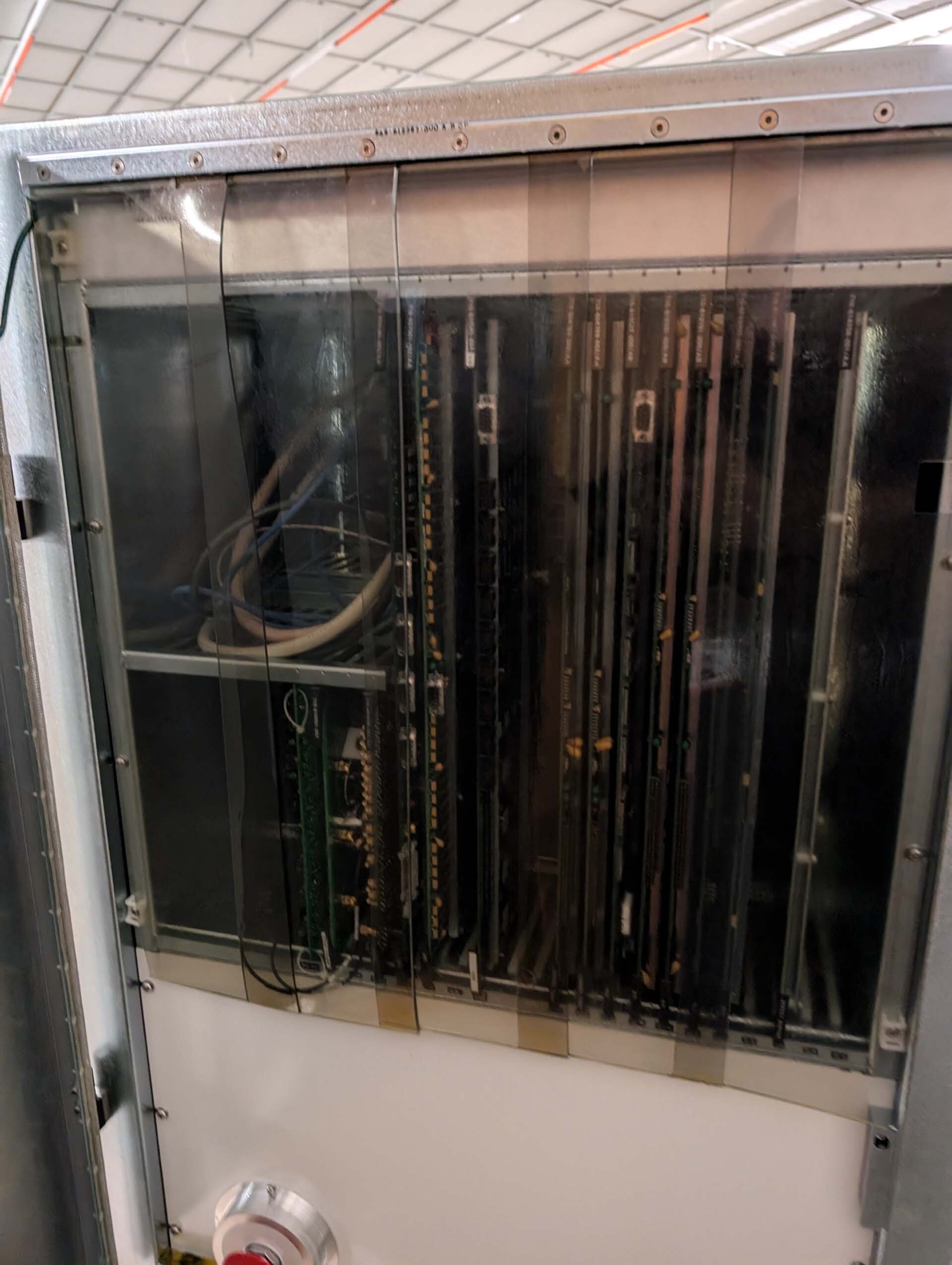
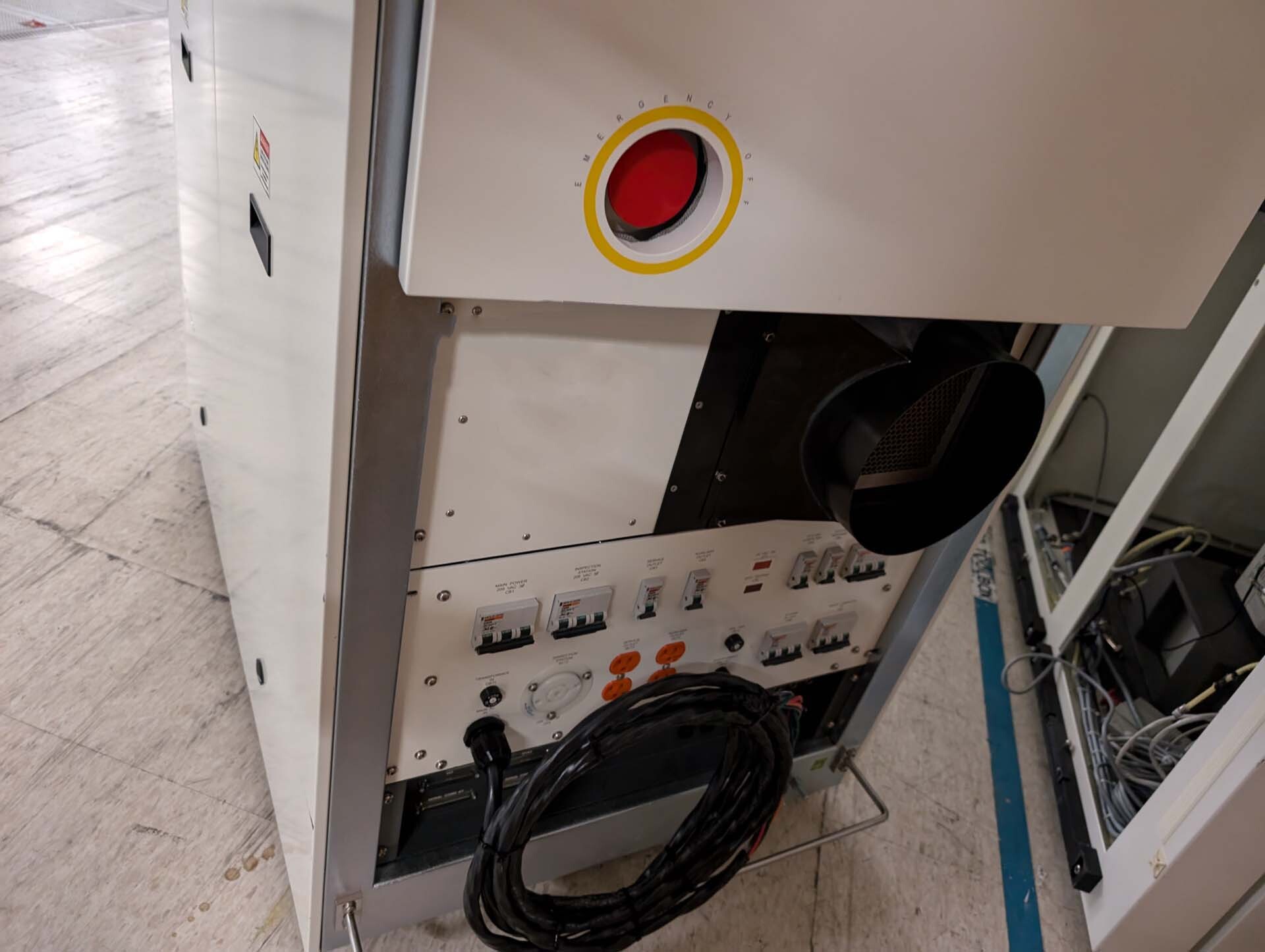
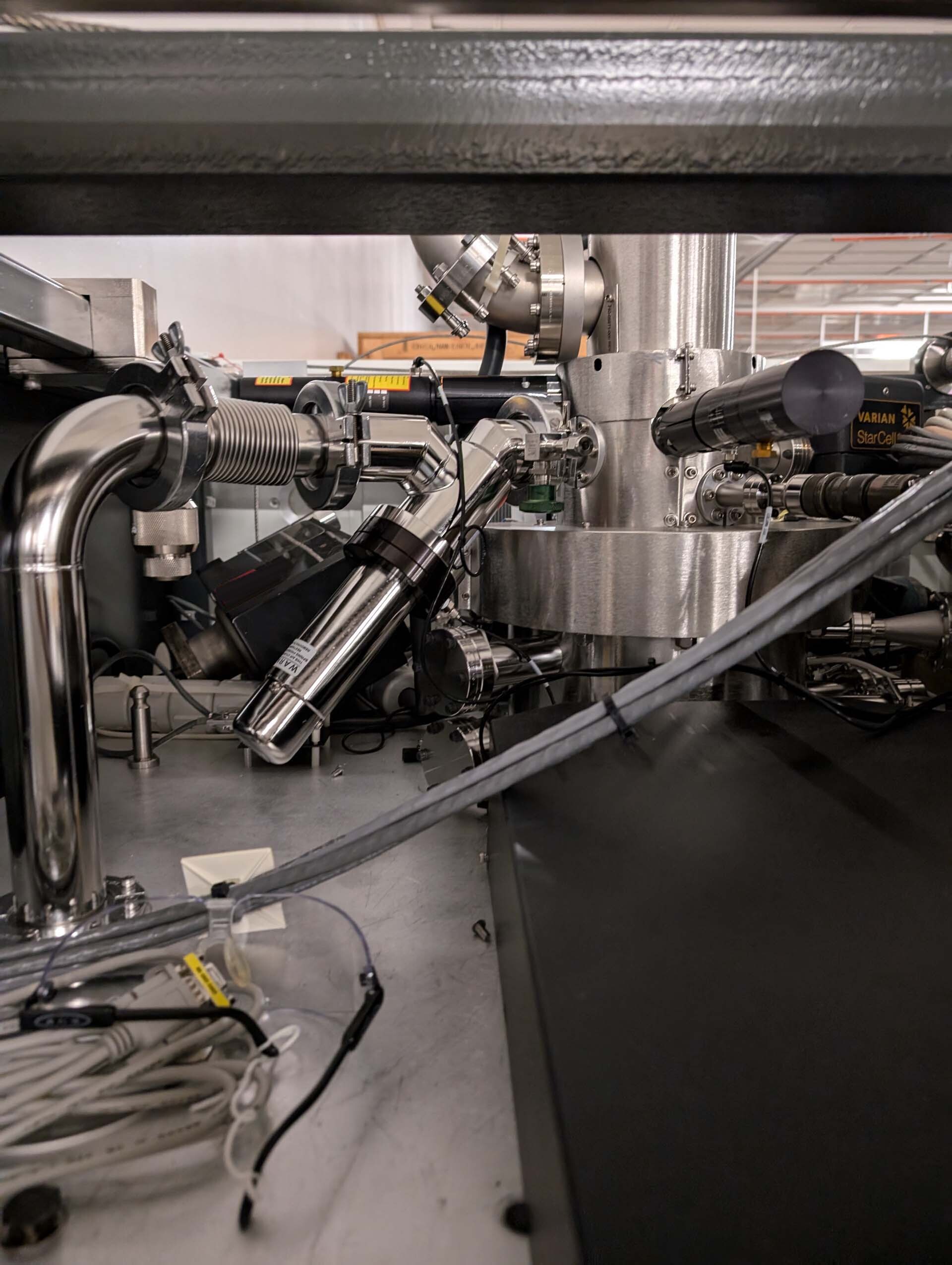
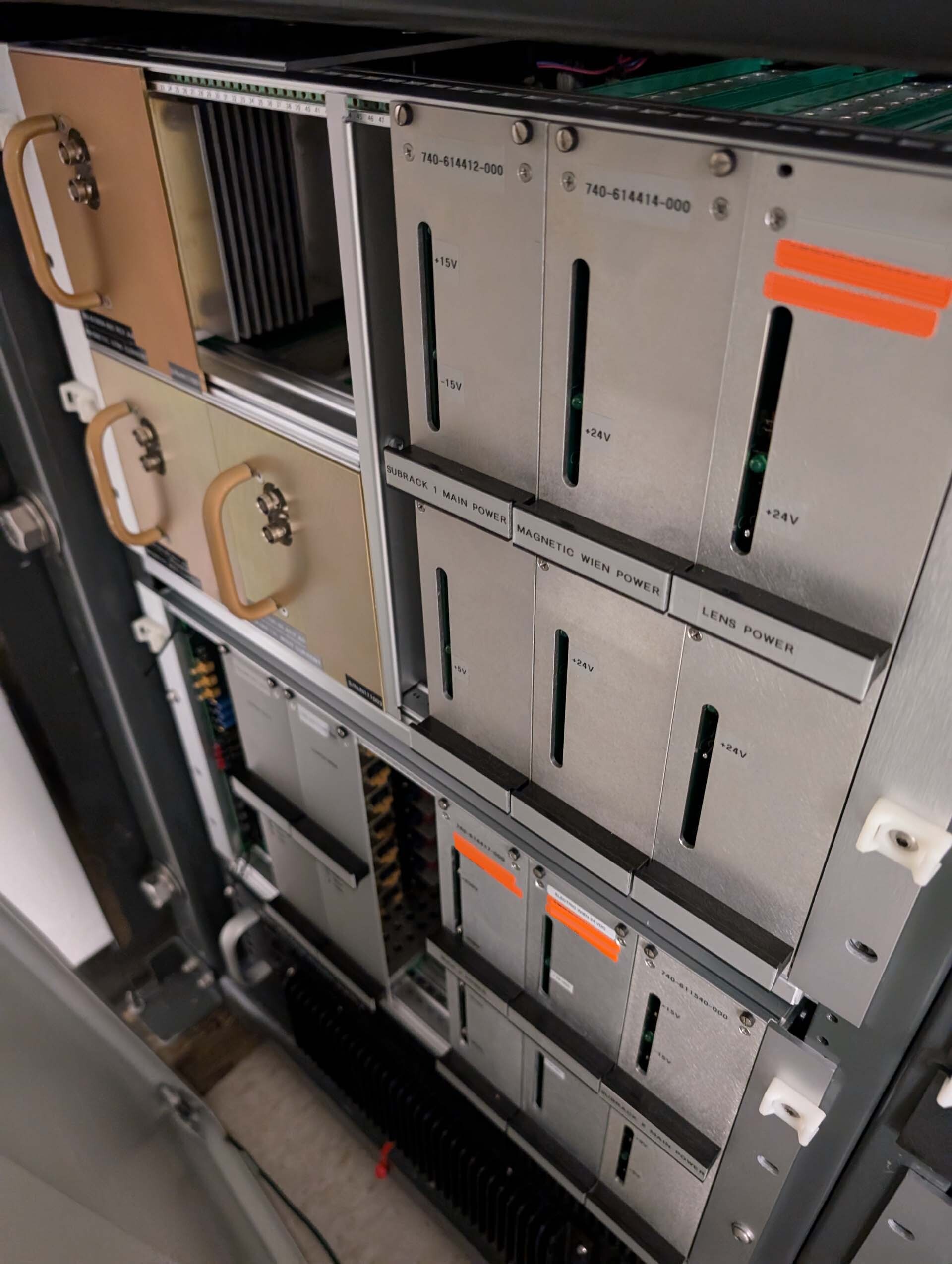
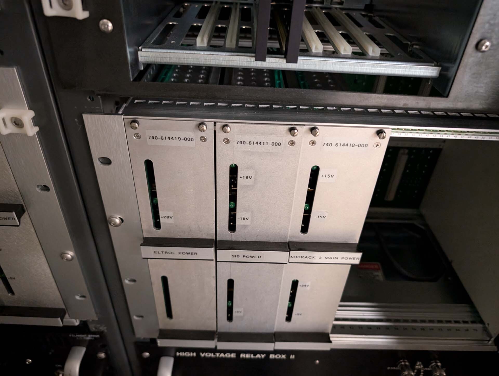
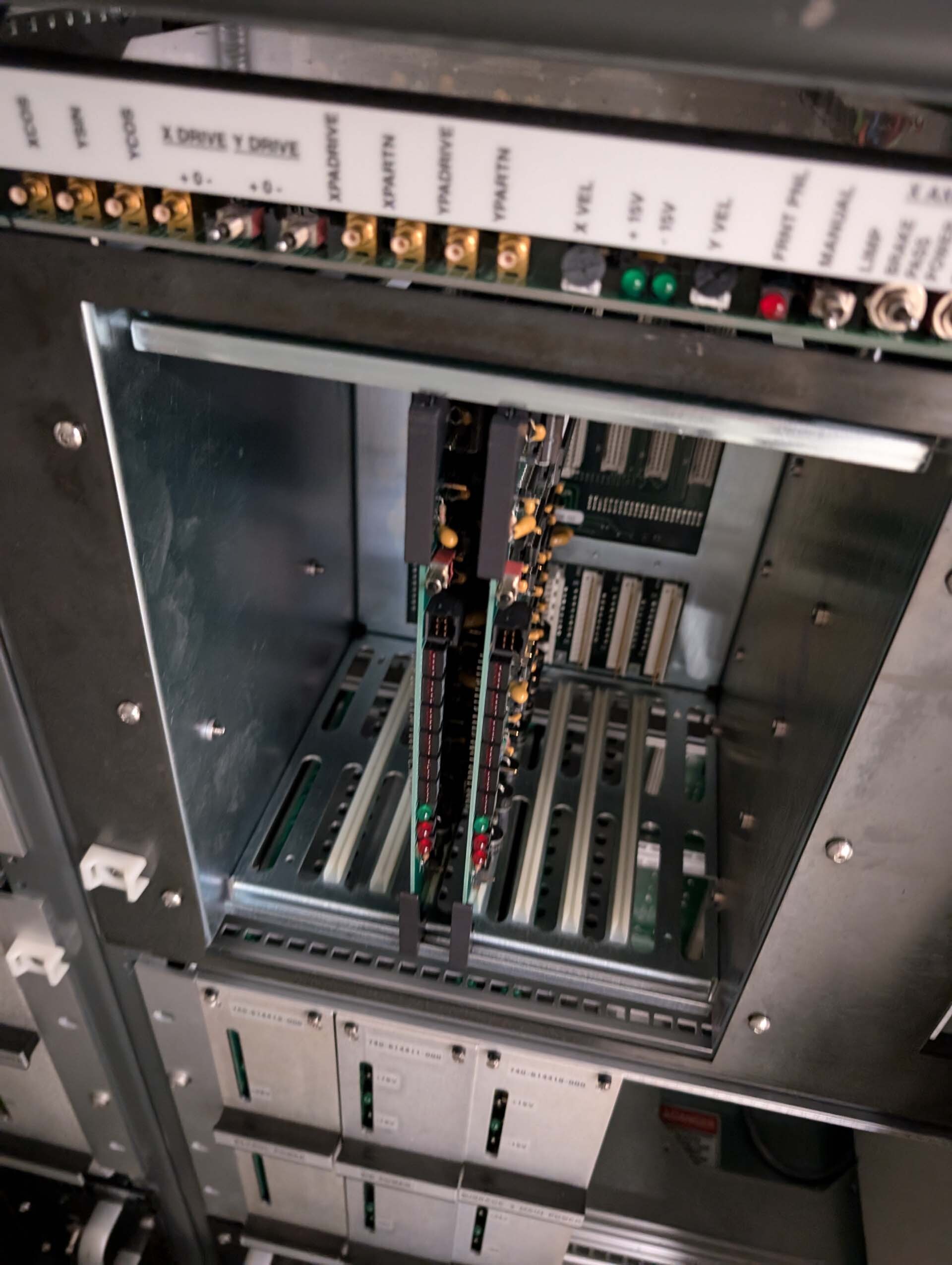
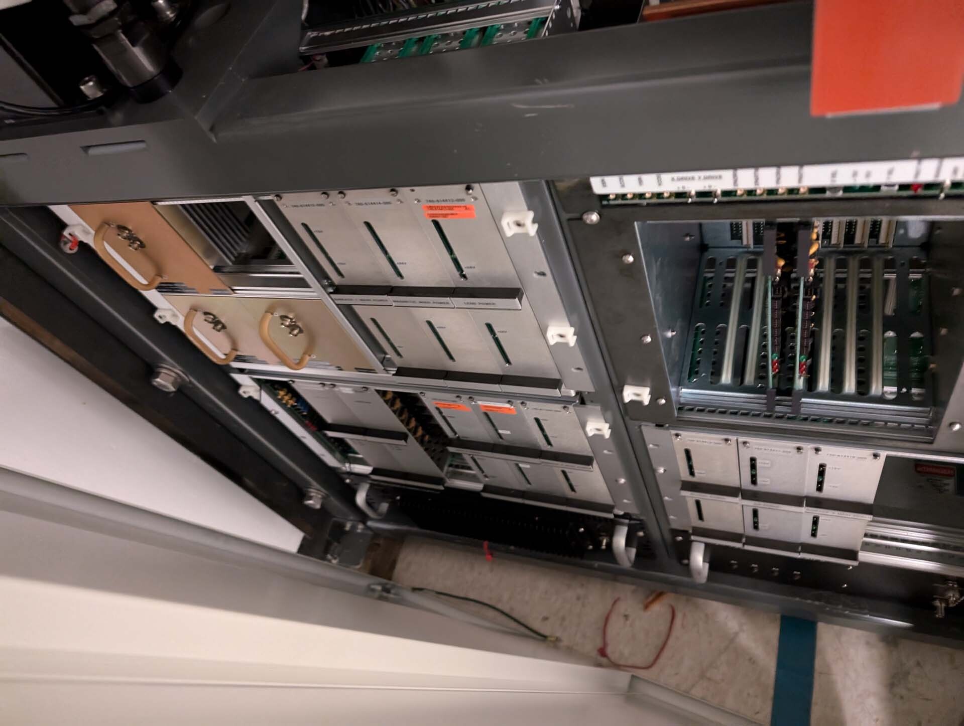
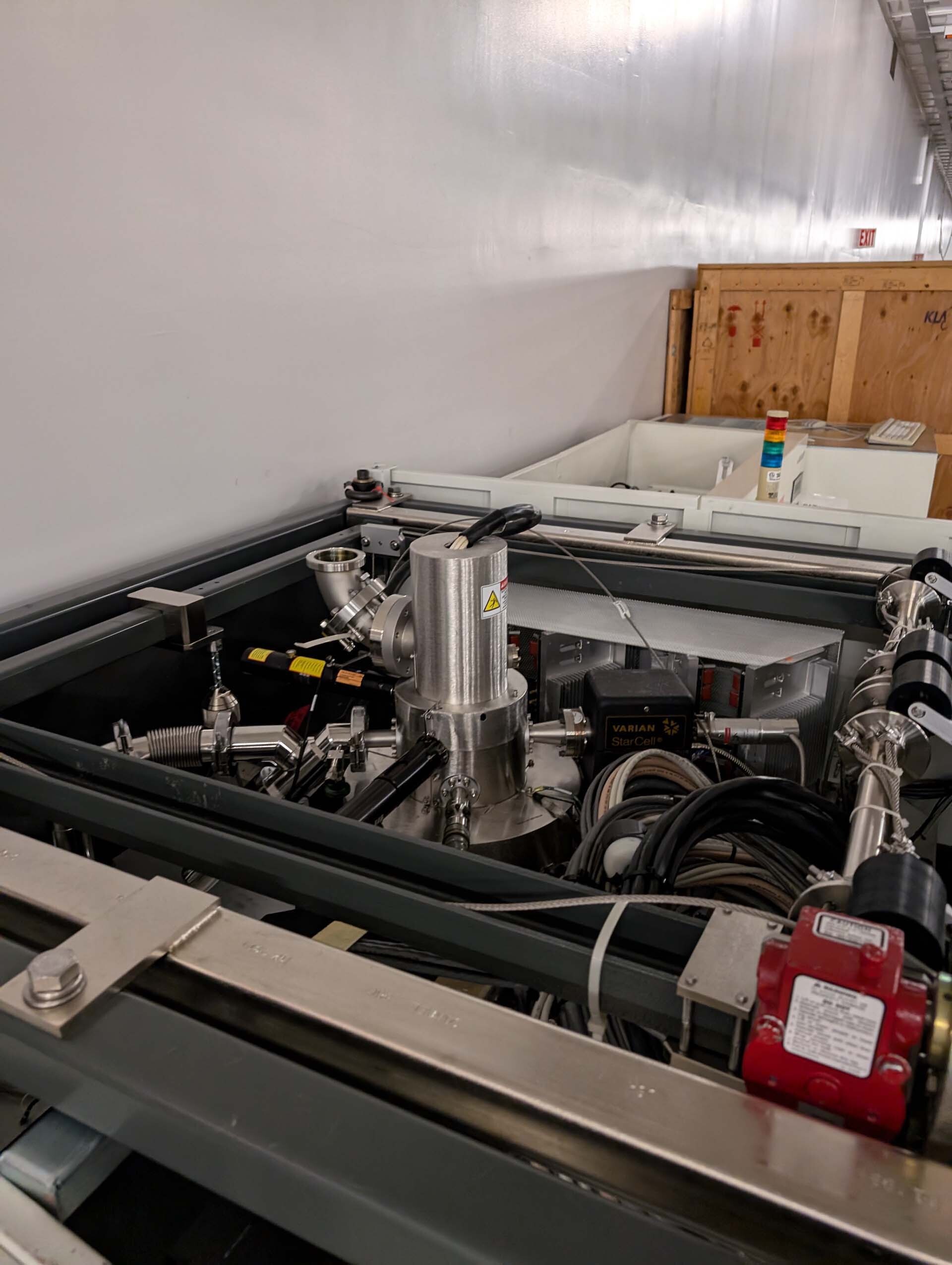
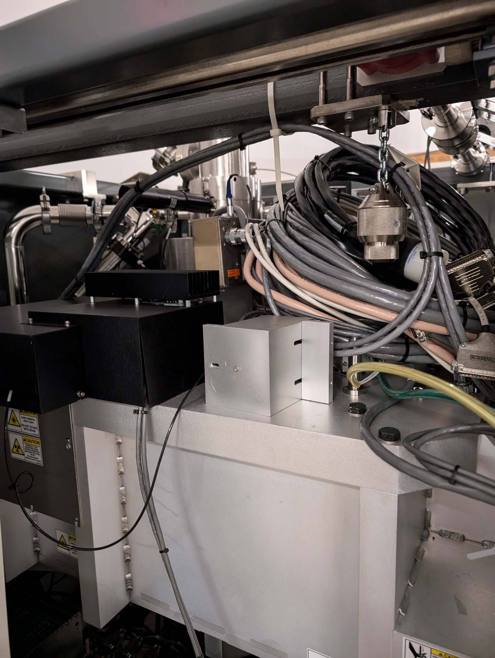
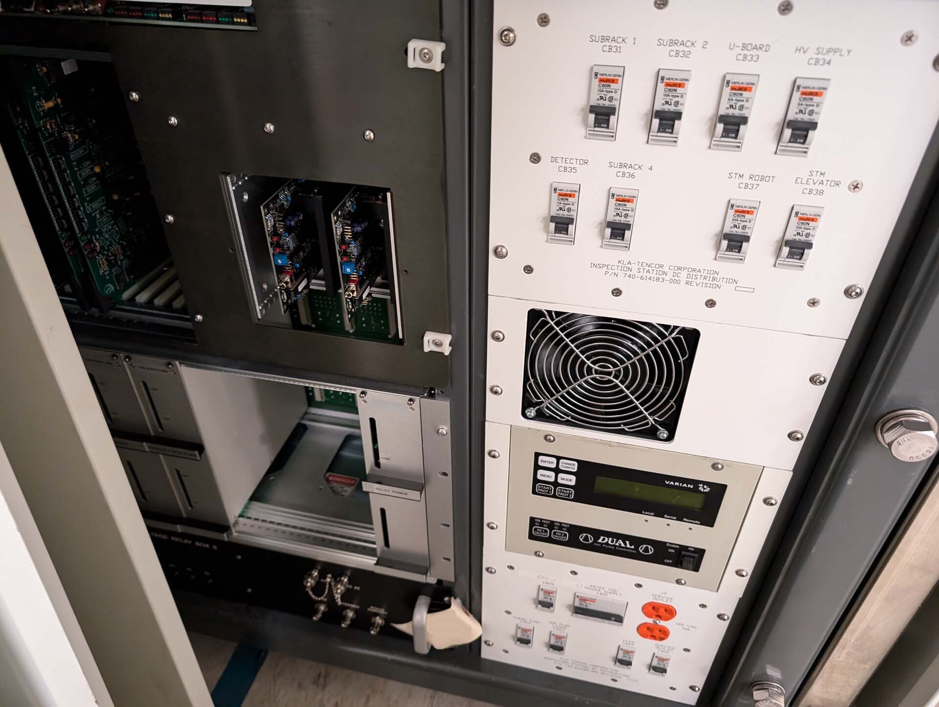
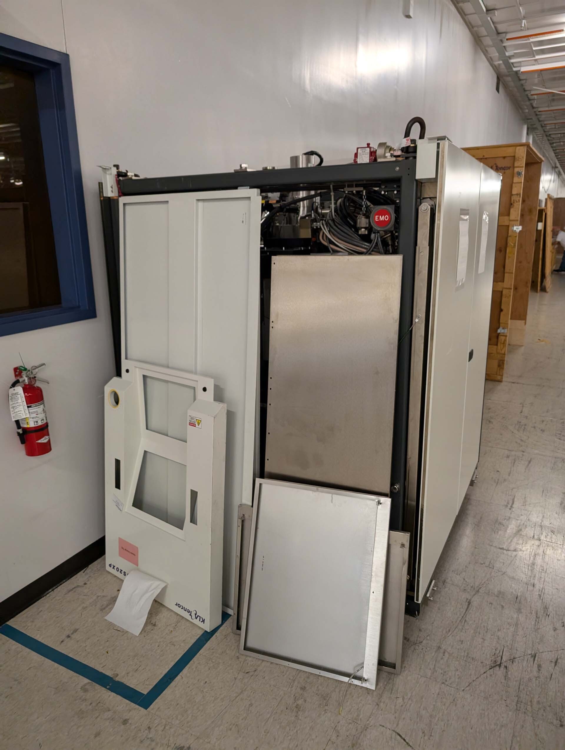
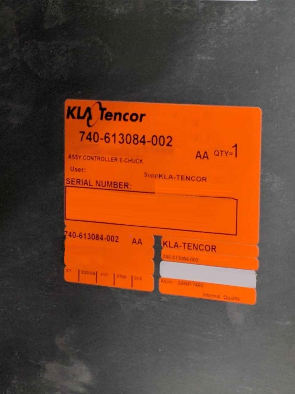
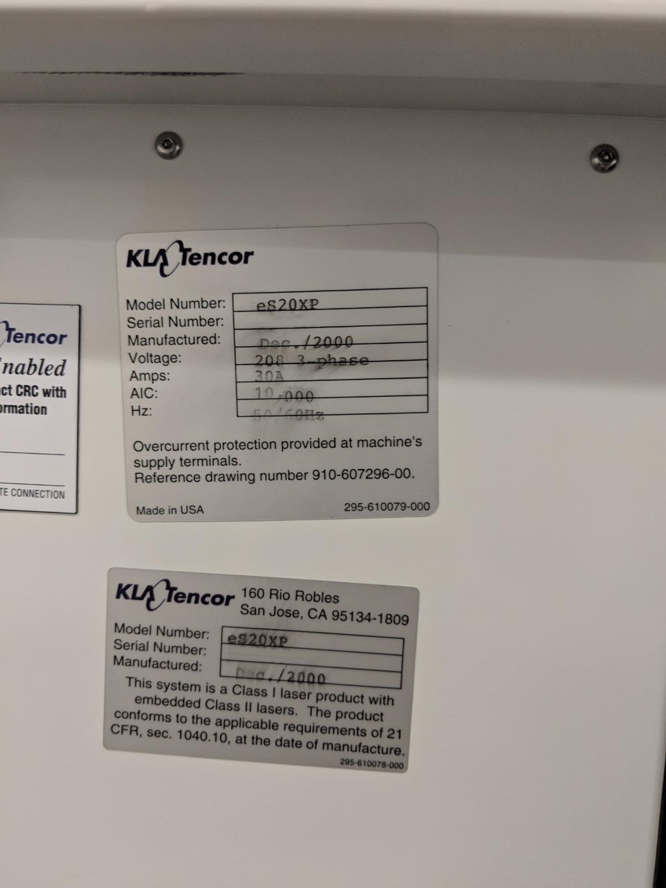
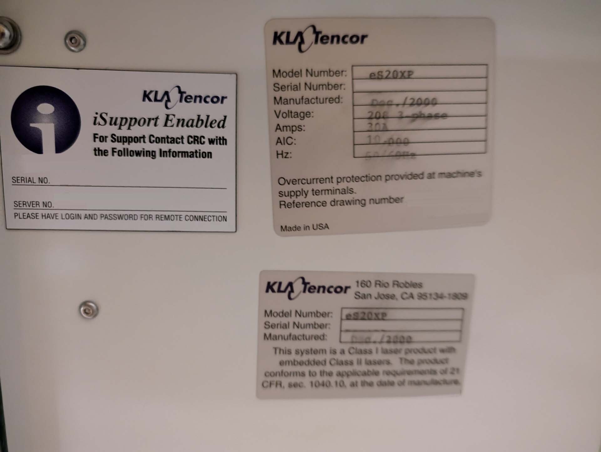
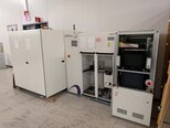
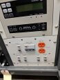
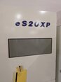
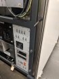
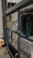
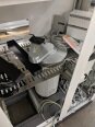
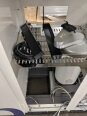
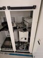
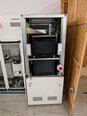
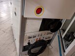
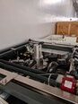
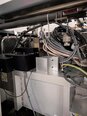
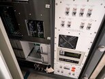
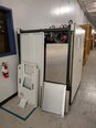
KLA / TENCOR es20xp is an advanced mask and wafer inspection equipment used in semiconductor device manufacturing. It enables the detection of defects in masks and wafers that may otherwise be undetectable using traditional inspection techniques. KLA ES20 XP system utilizes a combination of advanced optics and software to detect silicon defects down to the nanometer scale. This unit is capable of inspecting features on a wafer with a resolution of 5nm. With the use of a bright light source, TENCOR ES 20 XP helps identify defects with high contrast and unmatched repeatability. In addition, advanced software allows for KLA / TENCOR ES 20 XP to accurately detect foreign particles and imperfections. TENCOR es20xp utilizes optical microscopy techniques. This enables a clear, amplified view of the wafer's surface without the need for lenses or other optical components. The machine includes an autofocus tool that allows the user to quickly adjust the focus to different parts of the wafer, as well as an automatic gain asset which enhances the signal-to-noise ratio to provide a higher contrast image. KLA es20xp can be set to various scan modes. Single shot mode scans the entire wafer, while scan areas and scan fields can also be defined. With scan areas, a user can refine the scan and inspect particular locations on the wafer, while in scan fields, several different areas of the wafer can be inspected simultaneously. Finally, hot spot mode scans only areas that have high defect density. KLA / TENCOR ES20 XP can be used in a multitude of applications. It can be used to identify and correct die bonding issues, detect defects or damage to mask patterns, and evaluate surface morphologies of wafers. The model can be used in the detection of undercuts, shorts, voids, and scratches, as well as debris and failure sites. Es20xp is an advanced mask and wafer inspection equipment that enables detection of small defects and particles down to the nanometer scale. This system provides a high resolution view of the wafer's surface, allowing for fast and accurate defect detection. Various scan modes are available, allowing for the optimization of defect detection for high defect density areas. KLA ES 20 XP is an essential tool for semiconductor device manufacturers, enabling quick, reliable, and accurate inspection of masks and wafers.
There are no reviews yet