Used KLA / TENCOR SP1 Classic #9229734 for sale
URL successfully copied!
Tap to zoom


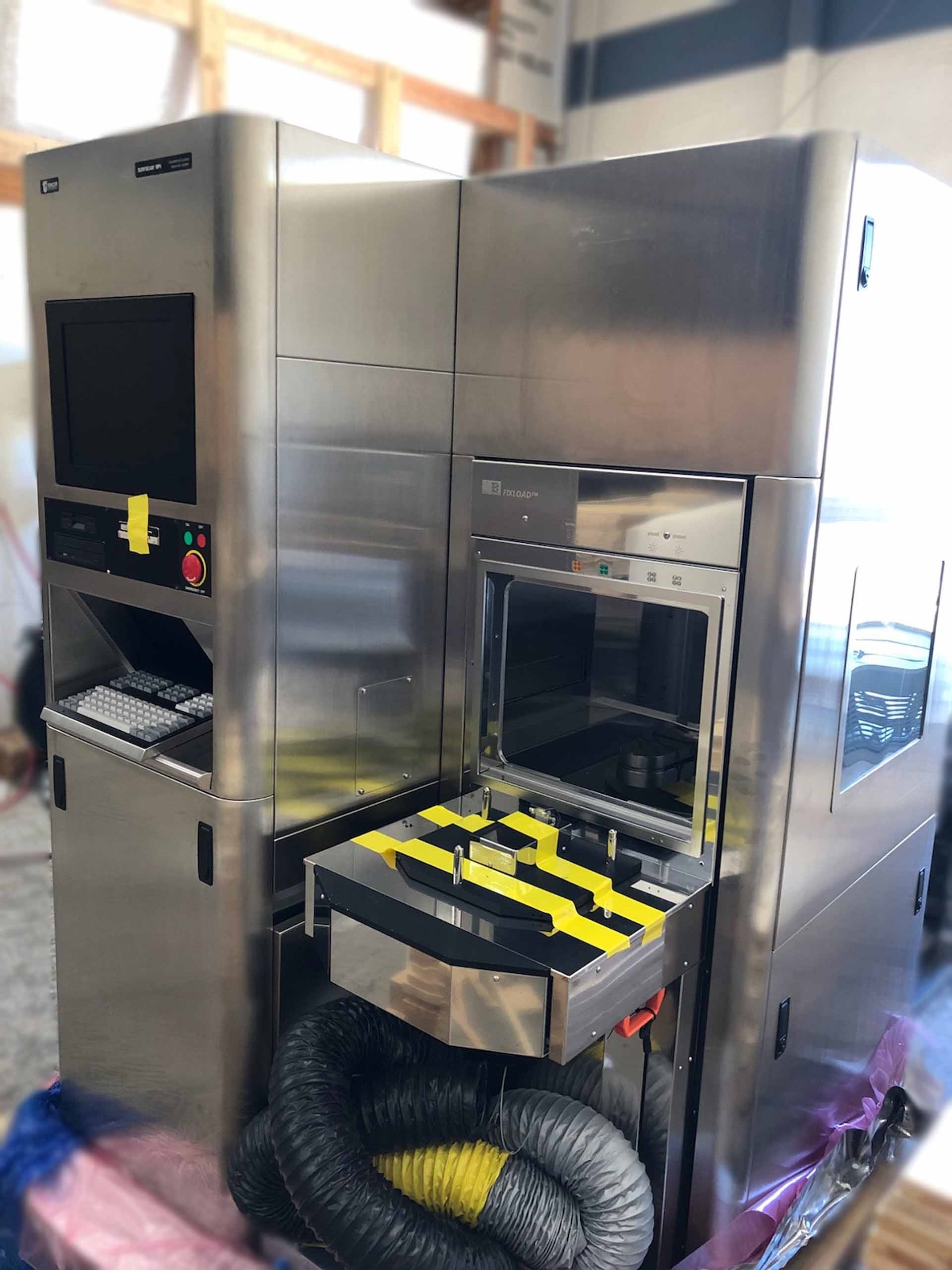

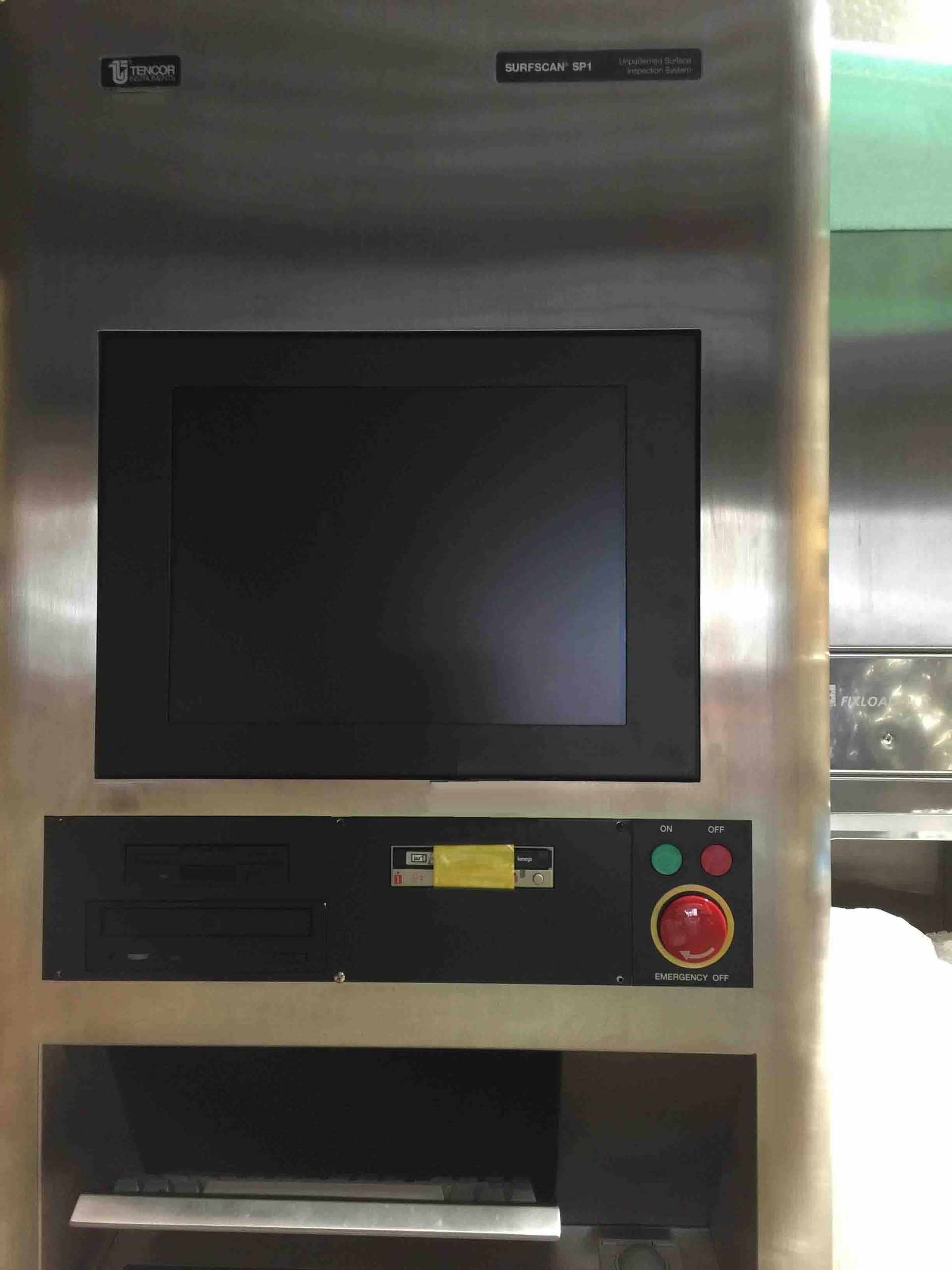

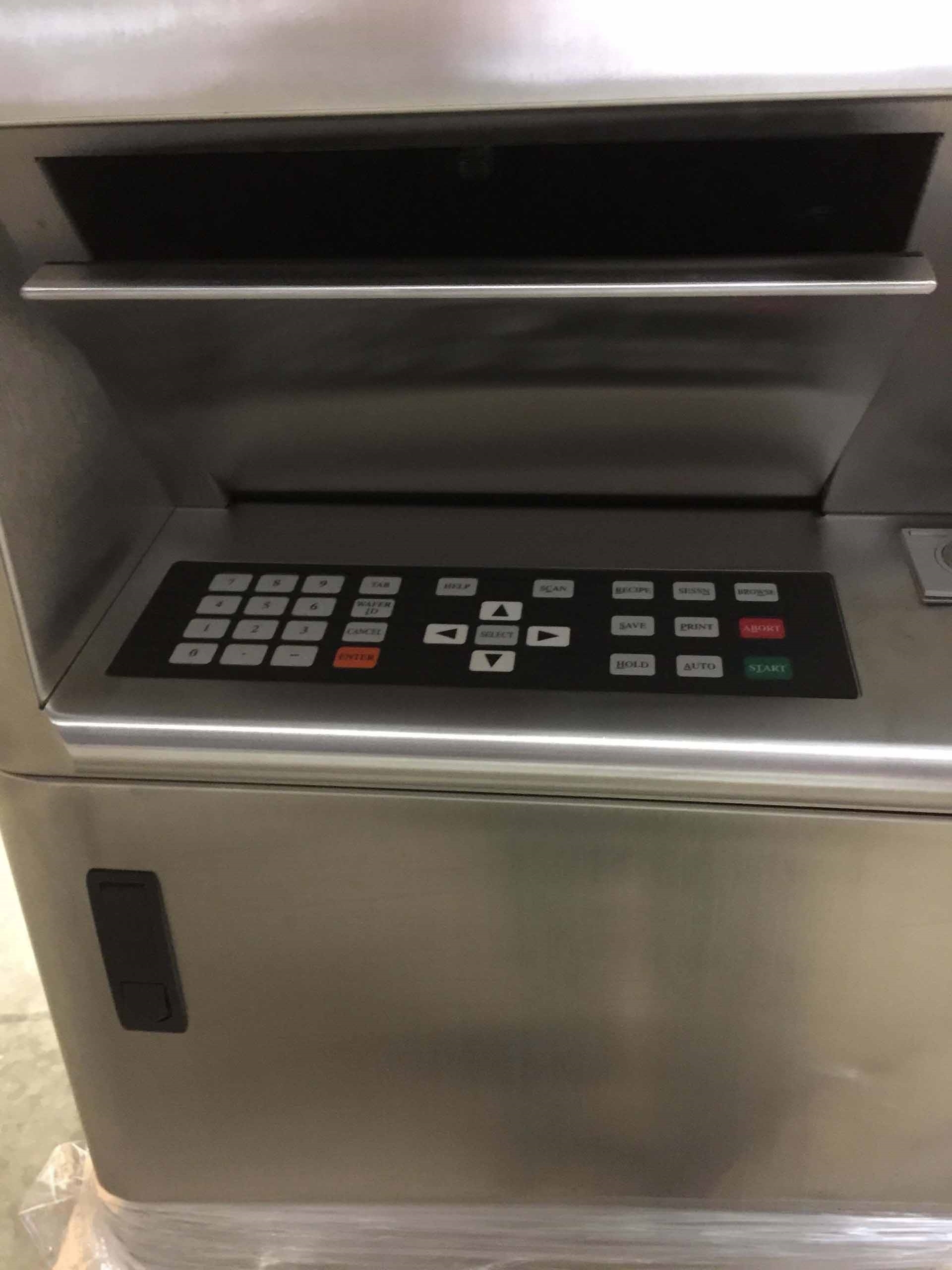


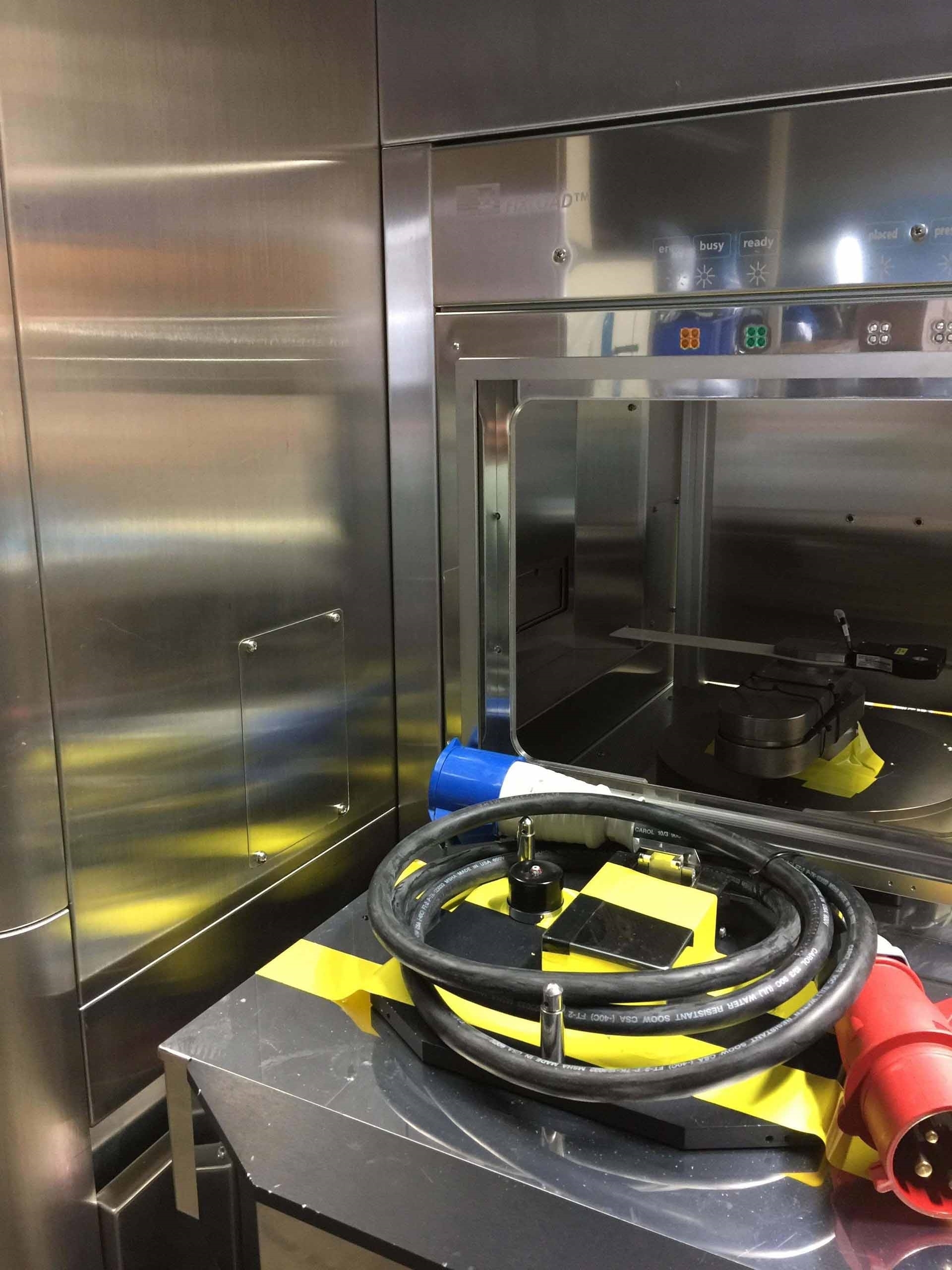

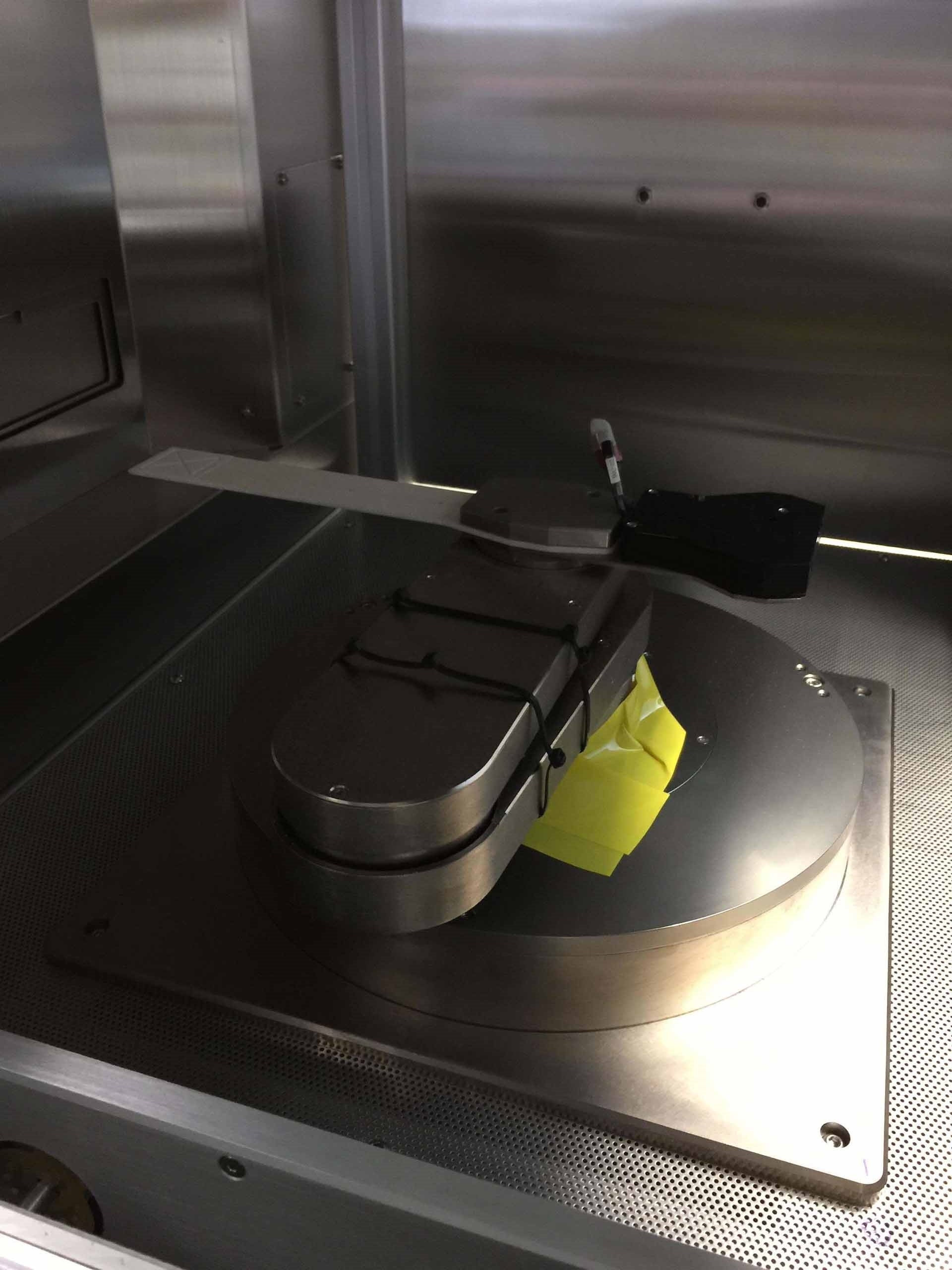

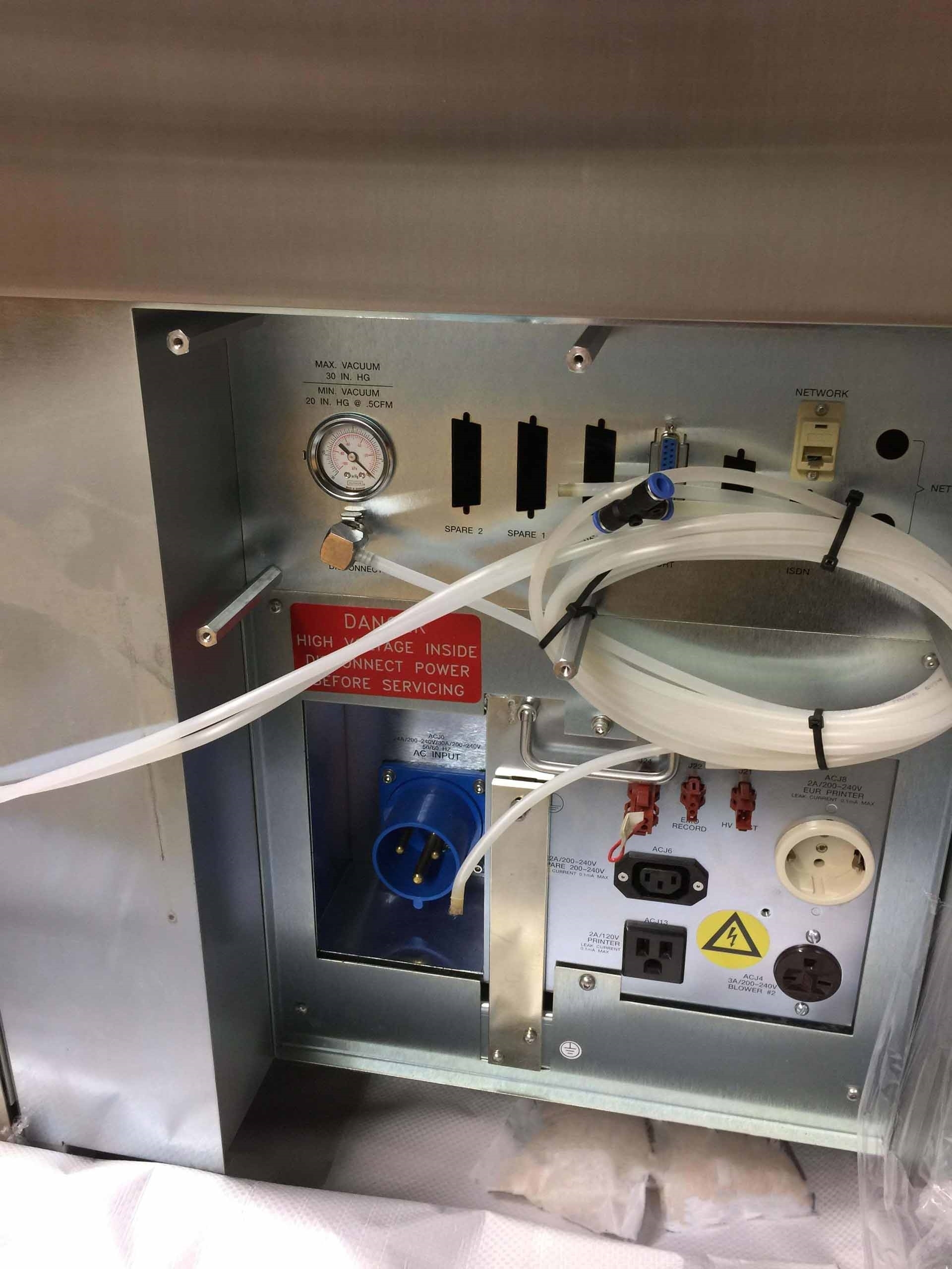

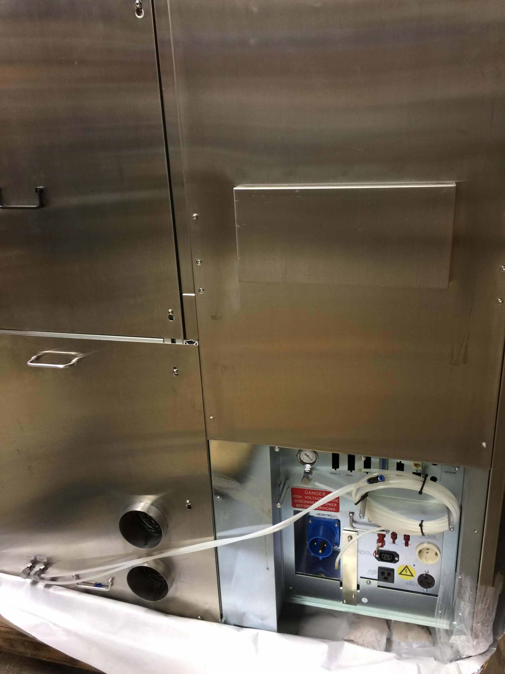

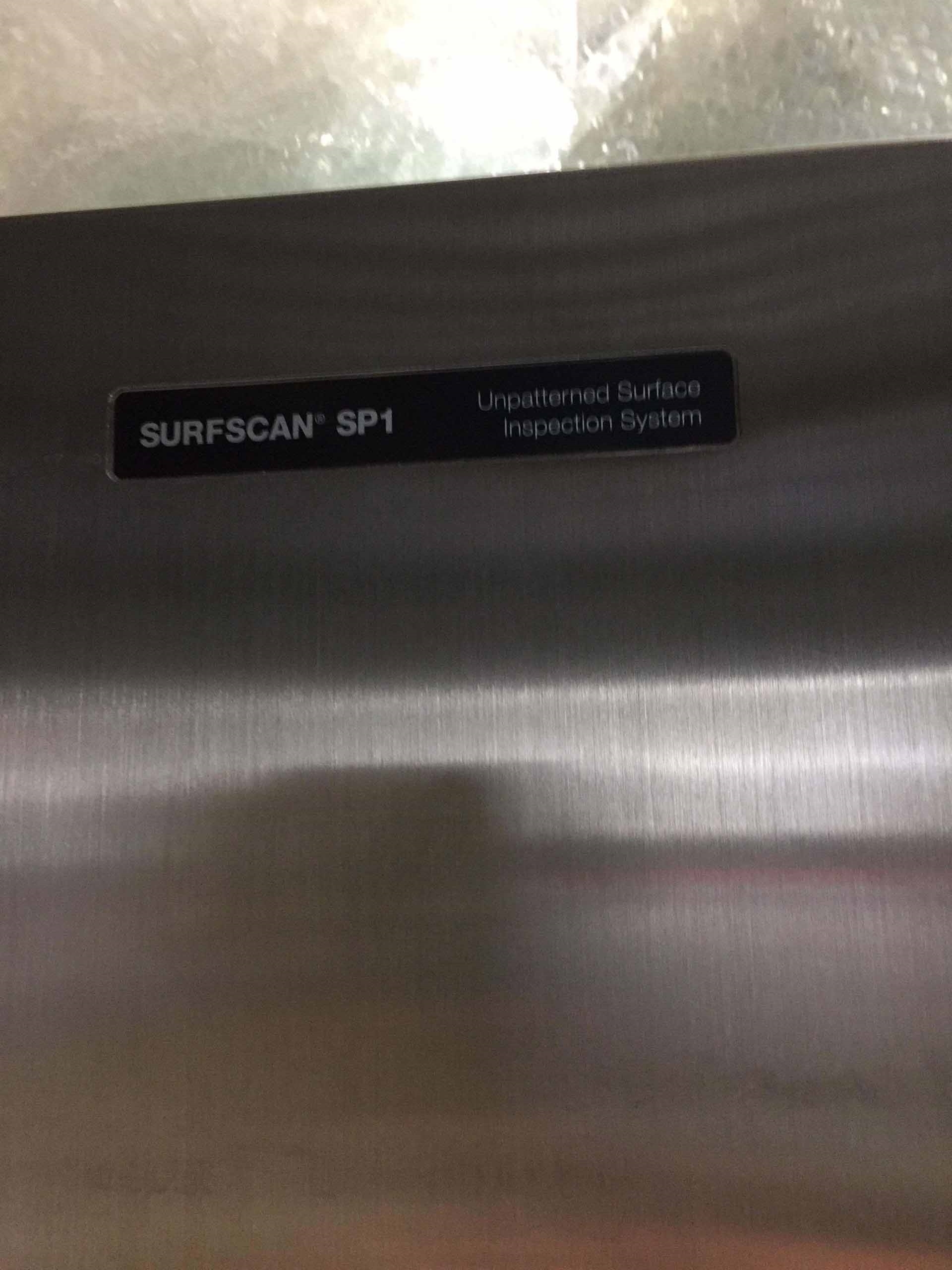


ID: 9229734
Wafer Size: 12"
Vintage: 1997
Inspection system, 12"
Single FOUP loader
Puck handling
1997 vintage.
KLA / TENCOR SP1 Classic mask and wafer inspection equipment is an advanced, non-contact optical pattern recognition-based inspection system used for a variety of 2D devices including chip layouts, lithography masks, printed circuit boards (PCBs), and in photomask inspection for integrated circuit (IC) manufacturing. It is designed to detect defects in structures ranging from small circuits to large chip arrays. KLA SP1 Classic provides high-speed, accurate pattern recognition, allowing users to quickly identify defects and anomalies in the mask or wafer. It offers high-resolution imaging with a maximum feature resolution of 0.3 μm, allowing it to detect small defects. Additionally, a high-performance data storage unit ensures fast, efficient data retrieval. For mask and wafer inspection, the machine comprises an advanced optical imaging microscope, beam splitters, calibrated laser and laser diode, linear linear-diode array detector, and digital image process computer. The microscope is equipped with a 12-inch square, high-resolution CCD camera. This produces an image of the mask or wafer, which is then projected onto the beam splitters. The two split beams are then focused and directed by a set of actively-stabilized mirrors. This creates an interference pattern, which is captured by the linear-diode array detector and transmitted to the digital image process computer. The digital image process computer then processes the interference pattern to identify defects in the mask or wafer. In addition to mask and wafer inspection, the tool can also be used for reticle acquisition. The reticle acquisition module helps ensure that masks and wafers are all accurately measured and inspected to get the most accurate results. Using TENCOR SP 1 CLASSIC mask and wafer inspection asset allows users to quickly and accurately check for defects in masks and wafers and significantly reduce manufacturing costs. Its high-resolution imaging and fast data retrieval capabilities make this model well-suited for a variety of applications.
There are no reviews yet


