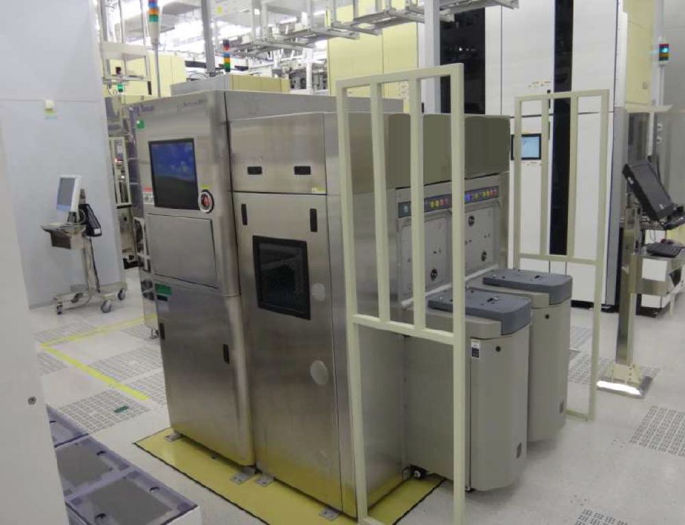
Used KLA / TENCOR SP1-DLS #9049192 for sale
It looks like this item has already been sold. Check similar products below or contact us and our experienced team will find it for you.
Tap to zoom


Sold
ID: 9049192
Wafer Surface Analysis System
Normal Illumination - 0.079Âum
Defect Sensitivity.0.005-ppm
Haze Sensitivity
Argon Ion Laser (488-nm)
RTDC (Real Time Defect Classification)
Measurement Chamber with ULPA Filter and Blower Unit
Operator Interface (integrated in Measurement Module)
Microsoft Windows XP 5.1 Operating System
Security, Logging & native Networking as provided by Windows XP
Interactive Pointing Device
Keypad Controls
TFT Flat Panel Display
Parallel Printer Port
Defect Map and Histogram with Zoom
MicroView Measurement Capability
Iomega 2GB Removable Jaz Drive
Operations Manual, Clean Room Book On Board, softcopy of SP1 Operations Manual
Software version 4.200
Hardware configuration:
Microsoft WinXP5.1
E40/E87/E90/E94
E84 enabled for OHT & AGV/RGV
GEM/SECS (Comm Port)
GEM/SECS (HSMS)
ASYST AXYS-21 Robot
300mm Dual FIMS Bulkhead Asyst
Two AdvanTag SingleWire CID
4 Color Light Tower
Brightfield.
KLA / TENCOR SP1-DLS (Scanning Probe 1- Defect Localization Equipment) is an advanced mask and wafer inspection system designed for comprehensive review of production and development wafers for semiconductor fabrication. It combines four different technology pillars - optical, electrical, scanning probe microscopy (SPM), and defect localization - to inspect, diagnose and localize defects on wafers and masks. The unit integrates high-resolution imaging of wafer surfaces with traditional wafer metrology and defect review. It enables directed defect review with sub-micrometre resolution - using Sub Resolution Assist Features (SRAF) to identify and localise clusters. A combination of automated process control to ensure quality and in-depth analysis for fault diagnosis provides reliable, performant wafer inspection. KLA SP1 DLS is equipped with an Automated Wafer Alignment (AWA) machine for easy and consistent wafer replacements. Its SPM Alignment Tool (SAT) minimizes the effect of wafer misalignment on imaging. TENCOR SP 1-DLS has a RAPIDTM Wafer Recognition Tool (WRS) which retrieves detailed process information for each wafer scanned. The data collected by the WRS is used to generate automated, high-resolution wafer maps from near mid-IR to deep-UV ranges. The wafer surface imaging on KLA / TENCOR SP1 DLS has sub-micron optical resolution across the entire wide field, and overlay performance of 1nm with detectability to 0.2nm. Its single shot 3D defect review offers greater detection results in less time, while the probability-based defect review allows for accurate defect localisation in 3D space. TENCOR SP 1 DLS works with a wide range of probing tools including Scanning Electron Microscope (SEM), X-ray and Electron Beam (E-beam). The SPM inspection enables up to 10um depth analysis for shallow trench isolation (STI), chemical mechanical planarization (CMP) and other local planar features. The defect classification tool is also available for locating feature defects. The Automated Defect Handoff (ADH) feature helps connect KLA / TENCOR SP 1 DLS to other imaging tools, such as scanning acoustic microscopy (SAM) and transmission electron microscopy (TEM). This enables a comprehensive wafer inspection solution. Overall, SP1 DLS is an advanced mask and wafer inspection asset designed to provide comprehensive defect review and diagnostic capabilities. Its combination of optical, electrical, SPM, and defect localization technologies allows users to inspect wafers with sub-micrometre resolution, detect and localize defects in 3D space, and access process information for each wafer scanned.
There are no reviews yet