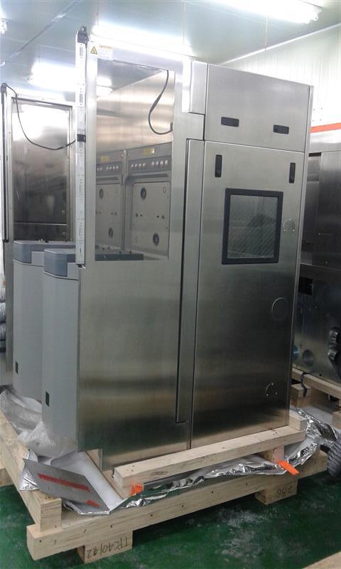
Used KLA / TENCOR SP1-DLS #9099729 for sale
It looks like this item has already been sold. Check similar products below or contact us and our experienced team will find it for you.
Tap to zoom


Sold
ID: 9099729
Inspection system, 12"
0.050um Defect sensitivity on polished bare silicon wafer
Normal illumination - 0.077 um defect sensitivity
Haze sensitivity - 0.005 ppm
Enhanced edge exclusion
Enhanced rough film sensitivity
75mW Argon ion laser (488-nm)
4 Dark field collection channels
RTDC(Real Time Defect Classification)
Dual-laser inspection
High-resolution haze information
The backside inspection module (BSIM) : Option
SW version 4.2 build 7179
Edge handling FLECWA
2nd UI option
2004 vintage.
KLA / TENCOR SP1-DLS Mask & Wafer Inspection Equipment is an automated imaging system designed to detect defects in semiconductor wafers as well as masks and films used in integrated circuit manufacturing. The unit employs a variety of advanced technologies such as brightfield, darkfield, and scatterfield imaging, and a range of specialised optical filters, enabling it to examine wafer surfaces and film thicknesses to a resolution of just 0.8μm. The machine consists of an inspection module which contains one or more wafer inspection ports, a series of illumination lamps and optics, and a suite of associated image acquisition and analysis software. The inspection port is a modular optical platform which can be configured according to the customer's requirements and application. It features a moveable x-y stage, a 20x to 1000x zoomable optical tool, and a ring-shaped brightfield illumination asset which enables the model to image even the smallest of features. KLA SP1 DLS equipment utilises a range of specialised optics that allow the system to be optimised for different kinds of defect detection. These include Transmissive Systems Optics (TSO) which uses two cameras to capture 2D images of wafers, and Reflective Systems Optics (RSO) which is optimised for the detection of defects on the surface of masks and films. TENCOR SP 1-DLS unit features advanced image analysis software which streamlines the defect detection process. Using sophisticated algorithms, the machine is able to detect the presence of defects in both brightfield and darkfield images. The tool can even detect defects that are invisible to the naked eye, such as particles and burned spots. Additionally, the asset has a high level of accuracy and repeatability, meaning that customers can be confident that it is accurately detecting any defects in a product. In conclusion, SP 1-DLS Mask & Wafer Inspection Model is an advanced automated imaging equipment designed to detect even the smallest of defects in semiconductor wafers, masks, and films. It employs a range of advanced technologies, including Transmissive and Reflective Systems Optics, and a suite of sophisticated image analysis software.
There are no reviews yet