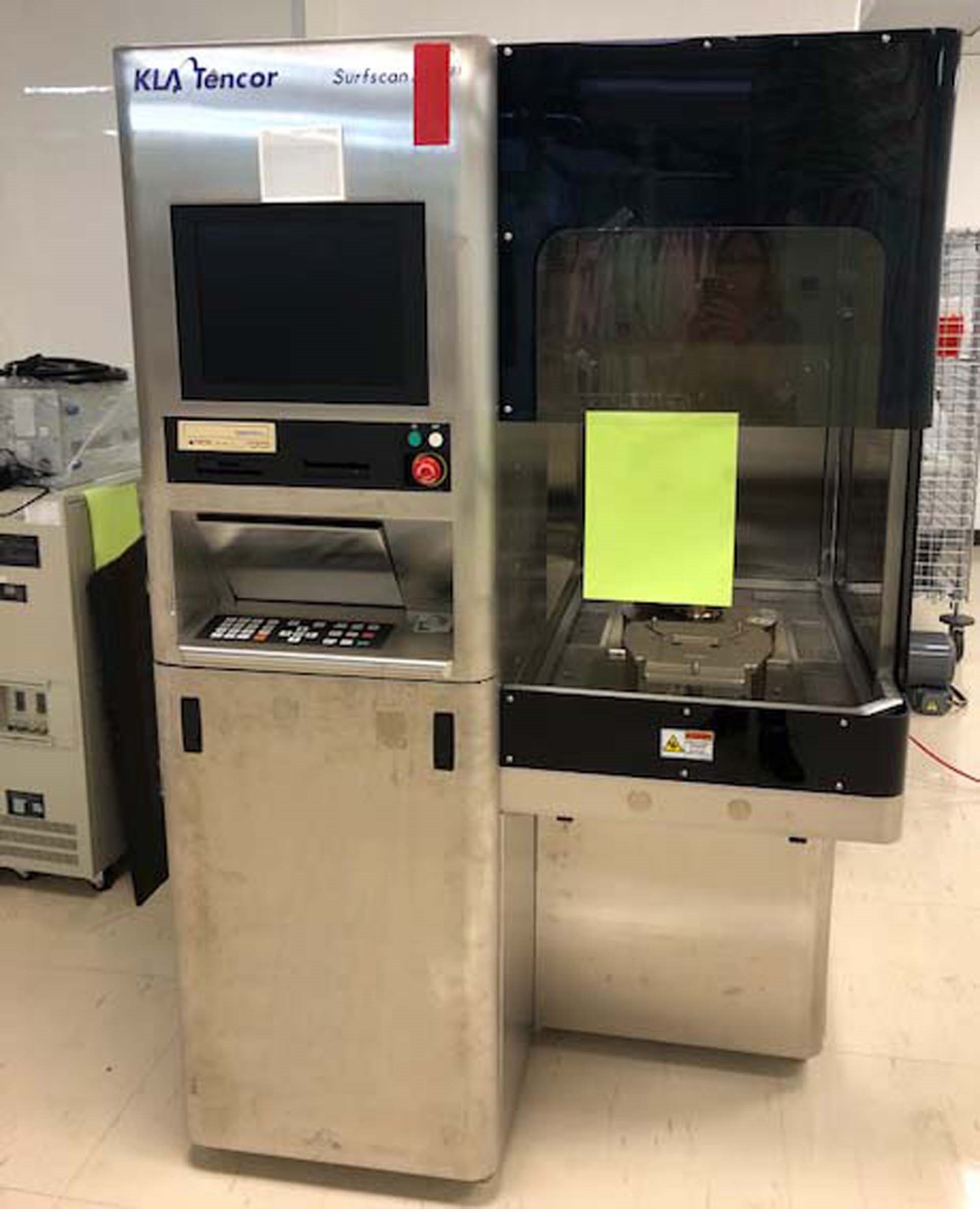
Used KLA / TENCOR SP1-TBI SURFSCAN #9235713 for sale
It looks like this item has already been sold. Check similar products below or contact us and our experienced team will find it for you.
Tap to zoom


Sold
ID: 9235713
Wafer Size: 8"
Vintage: 2000
Wafer particle measurement system, 8"
Install type: Stand-alone
Cassette interface:
Cassette station handler unit
Base plates, 8"
Brooks wafer handling robot
Mechanical movement cover (Tinted)
Main tool:
Vacuum chuck, 6" / 8"
Stainless steel paneling (Main & Handler units)
Twist-to-release EMO
Local user interface (Front):
Built-in keyboard
Mouse / Track-ball
Floppy disk drive: 3.5" (1.44 MB)
Drive: DVD-R/W
Accessories included: Blower unit
Facility requirements:
Vacuum
Exhaust
Missing parts:
SP1 Single puck assembly
Galil board
Motor drive cable, 60 pins
Y Motor
SP1-TBI, 6XXX, Tester, Laser & Argon, 30 MW
BF Analog PCB, TBI
BF Pre-amps, (2) TBI
BF DSP, TBI
Actuator SP1-TBI config
CD Pin set
Spindle motor power cable
DF Analog PCB, SP1-TBI
(2) DF Analog cables
LON Host PCB
Rocket port PCB
Hard disk drove
Laser power supply, TBI
Laser hose
Damage parts:
PWR1 Power supply
FFU Assembly SP1: Top & Front
Stage plexiglass cover
Panel, cover & bottom
Chuck wafer vacuum, 6"
(2) PMT Tubes
Track ball
CPU: 850 MHZ, SP1-TBI configured
Power supply: 208-240 VAC, 24 A, Single phase, 3-Wire, 50/60 Hz
2000 vintage.
KLA / TENCOR SP1-TBI SURFSCAN is an automated, high-precision mask and wafer inspection equipment designed for the semiconductor industry. The system has several essential elements that allow it to comprehend and interpret patterns of defects on silicon wafers and masks as well as observe and track uniformity attributes on the wafers. KLA SP1-TBI SURFSCAN unit includes the following components: High speed-scanning pattern recognition machine, which is capable of scanning and recognizing defects with a resolution of 65nm. This tool uses an algorithm that detects features while autonomously adjusting the number of sampling points in order to prevent over-sampling and under-sampling. Parallel mask inspection asset, which is capable of inspecting masks at high speed and aluminum and chrome layers up to 10 microns thick with a resolution of 25nm. Wafer inspection model, which includes an imaging equipment and several algorithms that are able to detect subtle deviations in the patterns on the wafer. This system also enables the user to adjust the size of inspected field and resolution Defect review and classification unit, which is capable of classifying defects on the basis of its position, shape, and intensity. Wafer trimming process control which ensures that trimming is done in an accurate and consistent fashion. Automated analysis and reporting machine, which allows the user to quickly generate detailed reports regarding wafer and mask defects. TENCOR SP1-TBI SURFSCAN tool is designed with safety protocols in place in order to ensure that contamination is not propagated during the operation. This asset also has the ability to be networked with other production systems such that all information concerning the scans and reports is readily transmitted and accessible. Overall, SP1-TBI SURFSCAN is an advanced mask and wafer inspection model, which is capable of quickly inspect and detect defects down to 65nm with high precision. With its integrated high-speed scanning and imaging components, the equipment can help maximize yields and ensure quality in the production of semiconductor products.
There are no reviews yet