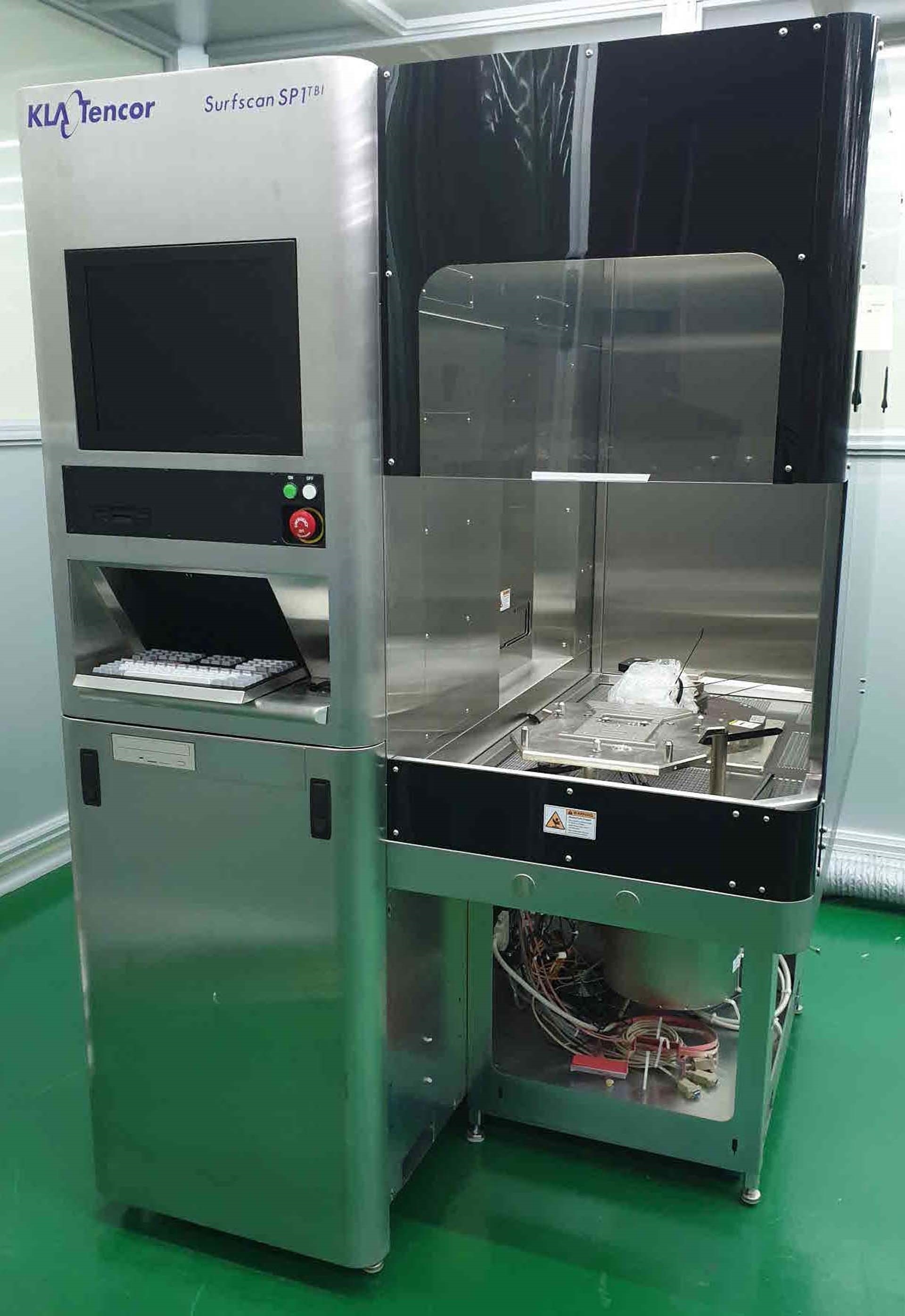
Used KLA / TENCOR SP1-TBI #9236208 for sale
It looks like this item has already been sold. Check similar products below or contact us and our experienced team will find it for you.
Tap to zoom


Sold
ID: 9236208
Wafer Size: 8"
Surface inspection system, 8"
Thickness: SEMI Standard wafer thickness
Defect sensitivity: ≤0.08 μm diameter PSL sphere equivalent ≥95% capture rate
Haze
Sensitivity: ≥0.005 ppm
Resolution: 0.0002 ppm
Repeatability:
Haze: CV ≤3.0% @ Avg. Haze 0.1 ppm
Count: CV ≤1.0% (Mean count 2000, 0.136 μm diameter latex spheres)
Sizing: CV ≤0.5% @ 0.136 μm histogram peak value
Edge exclusion: ≤ 1.0 mm for all wafer size
Spatial resolution: 20 μm spacing, minimum
Throughput
Standard: 80 wph for 300 mm @ 0.1 μm
120 wph for 200 mm @ 0.1 μm
150 wph for 150 mm @ 0.1 μm
Contamination: ≤0.001 particles/cm2/pass ≤ 0.12 pm
Cassette handling
Standard: Single puck w 1x300 / 2x200 mm cassette
Illumination source: 30 mW Argon-Ion laser, 488 nm wavelength
Operator interface: Keypad, trackball and keyboard standard
Operating system: Windows NT
Vacuum: < 20 KPa (≥ 24" Hg)
Electrical: 200-240V 50/60 Hz
Power Requirement: 5.4 kVA
Ducted venting: (2) 102 mm (4") exhaust hoses
Environment: Class 10 / Better.
KLA / TENCOR SP1-TBI is a mask and wafer inspection equipment that utilizes optical imaging, high-resolution imaging systems, and advanced defect detection algorithms. It is designed to detect even the most subtle defects on large-scale semiconductor devices. The system uses an LED-based quadruple-beam imaging unit with four times the resolution of conventional inspection systems. This allows it to detect even the most microscopic defects on a wafer or substrate surface. The machine also has automatic defect detection algorithms and image analysis software that can quickly and accurately detect defects. The tool is designed to scan samples quickly and efficiently. It is equipped with a high-speed vision asset to scan multiple layers of a substrate simultaneously. The model also has an automatic track optimization equipment which automatically readjusts the illumination of the sample depending on the current position. The system is extremely user friendly, as it has a customizable GUI and is compatible with a variety of software packages. It is also scalable, meaning it can handle both small-scale and large-scale semiconductor manufacturing tasks. The unit integrates with other KLA products such as the Contour Profiler, MultiDieEdge, and WaferTracker. These components provide a complete inspection solution for users. The machine also utilizes third party software packages such as IC Layout and Optimal Probe to ensure thorough and accurate inspection. KLA SP1T-BI also has several advanced features including programmable algorithms for customizing defect inspection patterns for a variety of sample types. It also includes a defect library which stores, reviews, and characterizes detected defects for future reference. Overall, TENCOR SP1 TBI is an advanced mask and wafer inspection tool that utilizes advanced imaging and defect detection technology. Its high-resolution imaging, customizable GUI, integration with third parties, and advanced features make it a powerful and reliable tool for detecting advanced defects.
There are no reviews yet