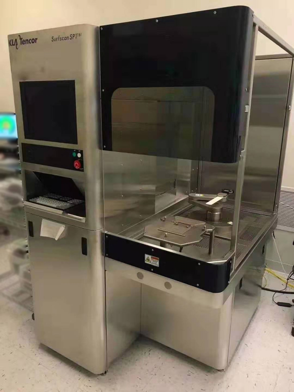
Used KLA / TENCOR SP1-TBI #9262812 for sale
URL successfully copied!
Tap to zoom


KLA / TENCOR SP1-TBI is a Mask and Wafer Inspection Equipment designed for the inspection of advanced semiconductor devices. The system has a high throughput capacity and is capable of inspecting wafers up to 200 mm in diameter, and up to 200 mm in thickness. KLA SP1T-BI also has an advanced optical unit for the detection of defects on masks and wafers. The machine has a laser confocal imaging tool, which is composed of a laser illuminator, an objective lens, and a camera. The laser illuminator provides a high-resolution image of the wafer and mask. The objective lens focuses the laser light on the wafer and mask, while the camera captures the image. TENCOR SP1 TBI asset has a comprehensive suite of metrics to measure and analyze defect parameters on the masks and wafers. These metrics include defect size, shape, position, brightness, and contrast. SP 1-TBI can also quickly detect and measure defects on mask side walls, which can be used to reduce the potential for downstream manufacturing defects. The model is equipped with an automated pattern recognition algorithm, which can quickly analyze and identify defects on the mask and wafer. For optimum inspection performance, TENCOR SP1-TBI offers several options for image processing. The equipment has an imaging processor, which can improve the system's imaging performance by adding filtering, noise reduction, and other image enhancement capabilities. Additionally, SP1-TBI has built-in algorithms for automated detection, classification, and characterization of defects on the masks and wafers. The unit also supports automated image segmentation, which enables users to segment the defect image into multiple regions for further analysis. KLA SP1 TBI machine offers several tools for automated operation and data analysis. The tool has the ability to store and manipulate inspection data, as well as display results in various formats. Additionally, KLA SP 1-TBI has tools such as an automated defect region identification utility and a particle counter utility. These tools can be used to quickly identify defects on the mask and wafer and automatically convert the defect regions into numeric data for further analysis. SP1T-BI's advanced imaging and inspection capabilities, coupled with its automated tools for defect characterization and analysis, make it an essential inspection asset for inspecting advanced semiconductor devices. With its impressive throughput, high resolution, and comprehensive suite of metrics, SP1 TBI provides users with the tools they need to analyze their masks and wafers for potential defects.
There are no reviews yet