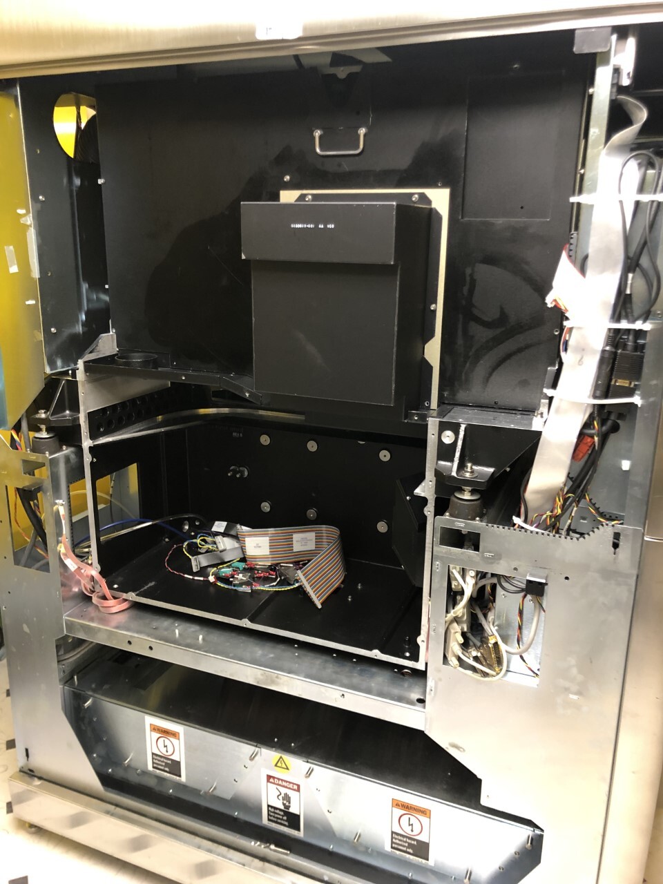
Used KLA / TENCOR SP1 #9407601 for sale
It looks like this item has already been sold. Check similar products below or contact us and our experienced team will find it for you.
Tap to zoom


Sold
KLA / TENCOR SP1 is a mask and wafer inspection equipment designed to help detect defects on photomasks and wafers in the semiconductor manufacturing process. This system utilizes sensor technologies, imaging systems, and data analysis techniques to obtain the most precise, high-resolution images of the various structures present on the wafer or mask surface, as well as of original features on the wafers. The systems are available in various configurations, allowing a wide range of imaging capabilities and functions, such as: overlay measurement; mask alignment; CD-SEM; Critical Dimension scanning; micro-defectivity mapping; CD and overlay CD control; Masking and OPC control; comparison of scan data to CAD; and defect inspection. KLA SP1 unit is equipped with four distinct imaging sensors: two electron beam detectors, one scanning laser detector, and one focus beam detector. The electron beam detectors generate high-precision images that enable precise analysis of tiny features and defects on the surface. The scanning laser detectors produce images of larger structures, helpful for detecting surface defects and examining the general condition of the wafer or mask. Finally, the focus beam detects imaged fine structures, with the highest accuracy focusing capability of all the imaging sensors. The machine is also equipped with an intelligent data analysis package that helps operators better interpret images produced by these imaging sensors. This advanced analysis package employs various algorithms and technologies to identify various features and variation within the image, and then provides an output that simplifies inspection processes. It is especially useful in detecting subtle changes and flaws on different levels, such as surface topography and sub-cell features. Data generated by TENCOR SP 1 tool is further enhanced with Advanced Process Control (APC) tools, which help operators and engineers identify defects, predict problems, and carry out complex analysis tasks. This can increase production and inspection yields, reduce cost, and optimize the workflow in the semiconductor manufacturing process. SP 1 asset has been used in many semiconductor device production lines, and has proven to be a reliable and powerful tool for managing defect-critical semiconductor manufacturing processes. It is an invaluable tool for achieving the highest possible production yields and maximizing returns on investment.
There are no reviews yet