Used KLA / TENCOR SP2 #9099730 for sale
URL successfully copied!
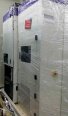
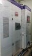

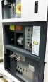
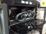
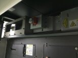

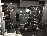
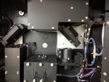
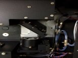
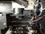
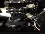
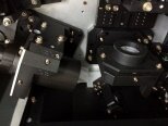



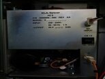

Tap to zoom
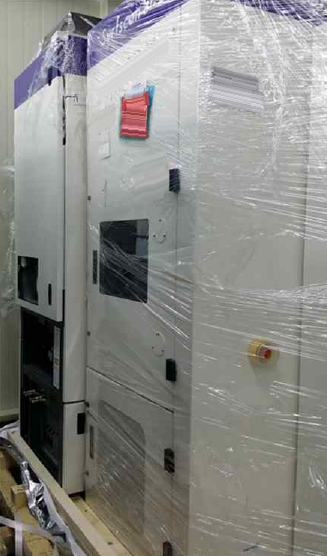

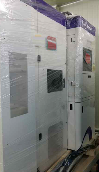
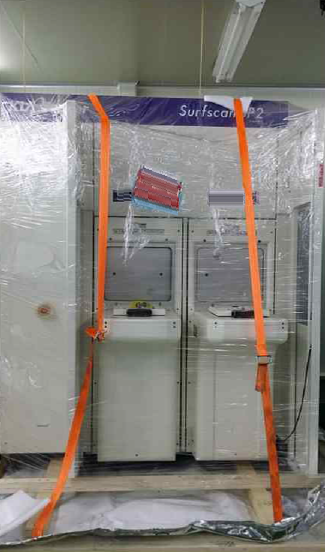
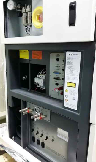
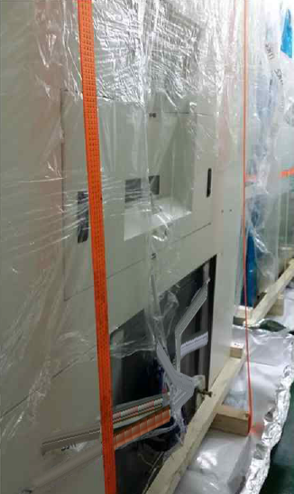
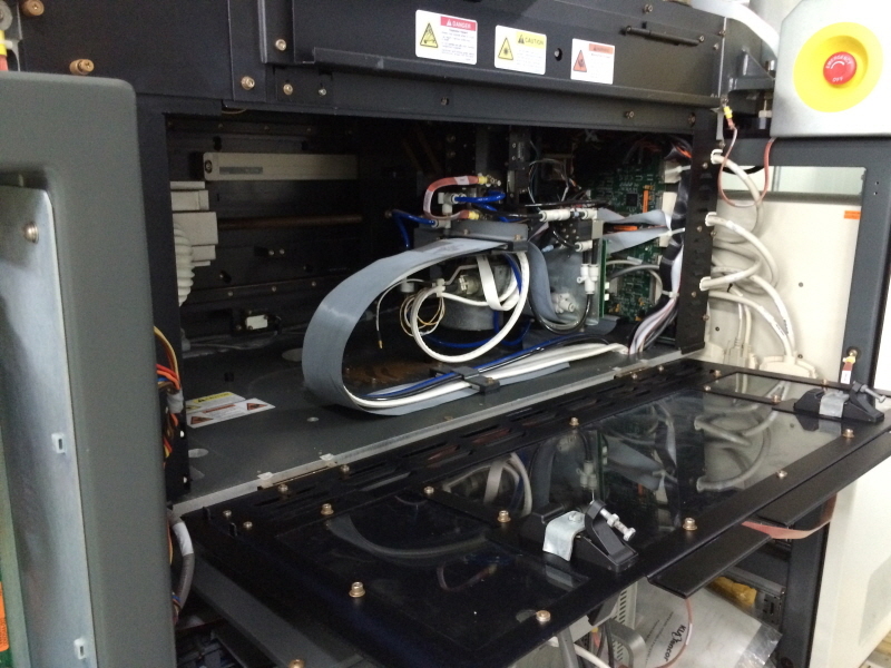
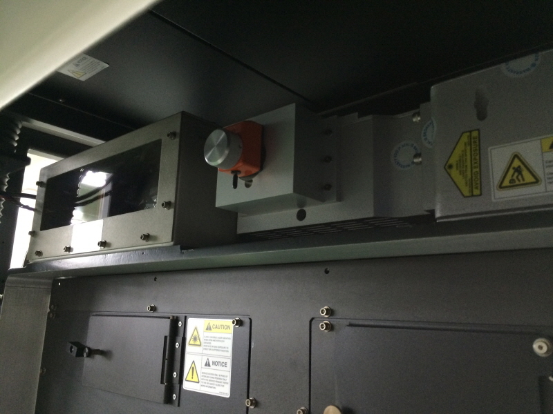
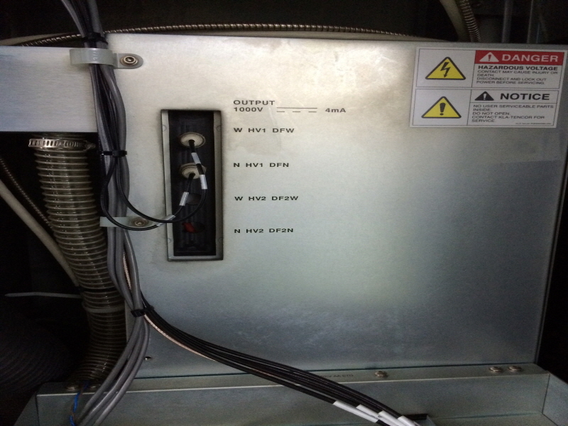
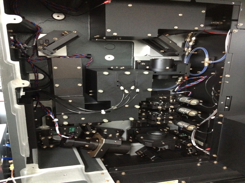
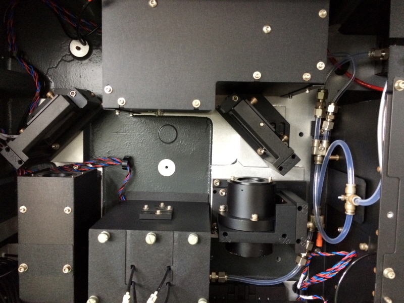
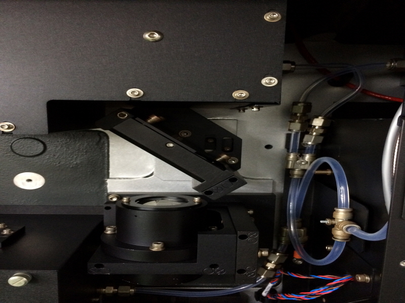
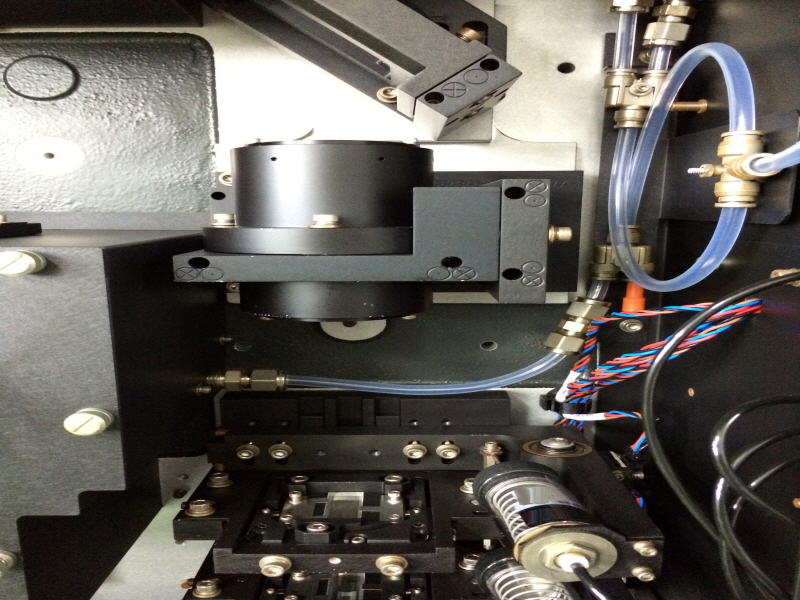
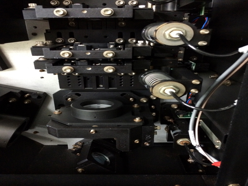
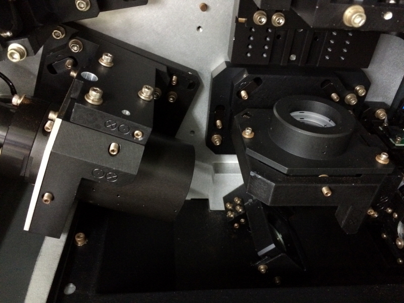
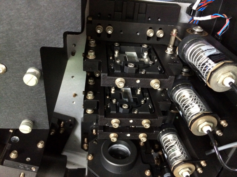
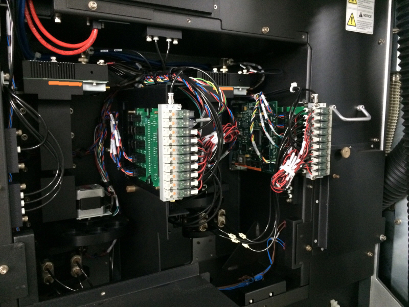
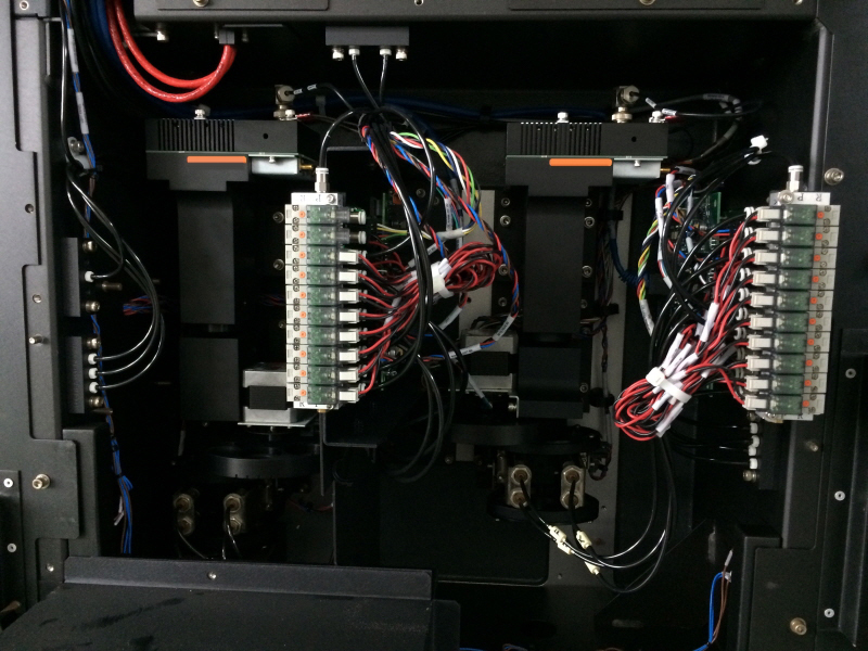
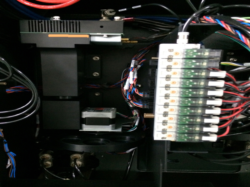
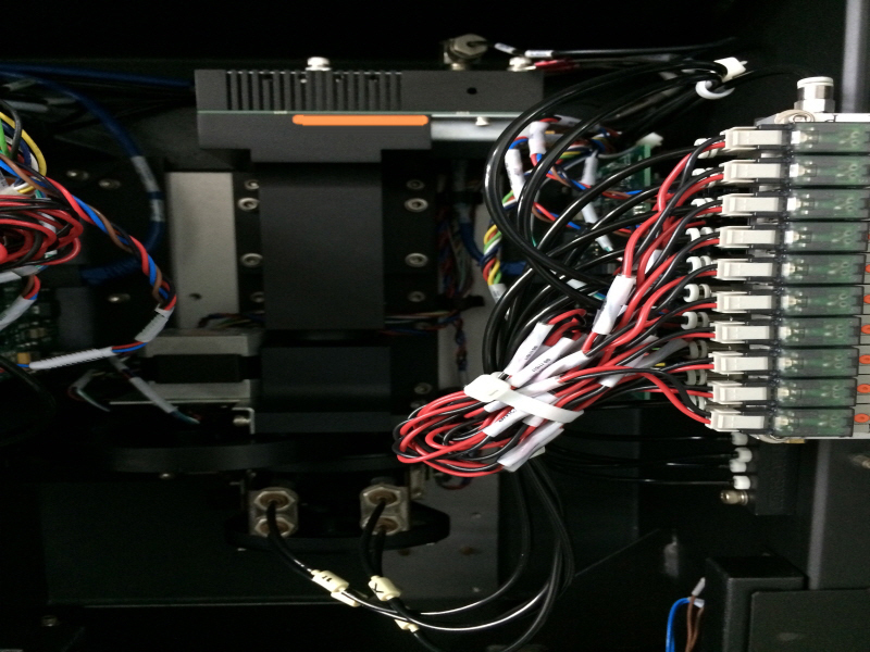
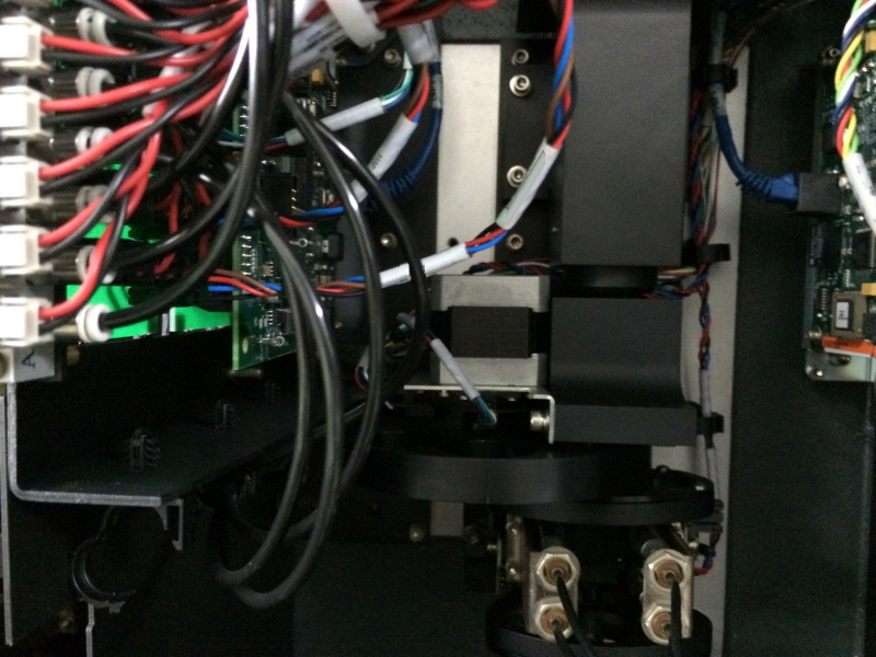
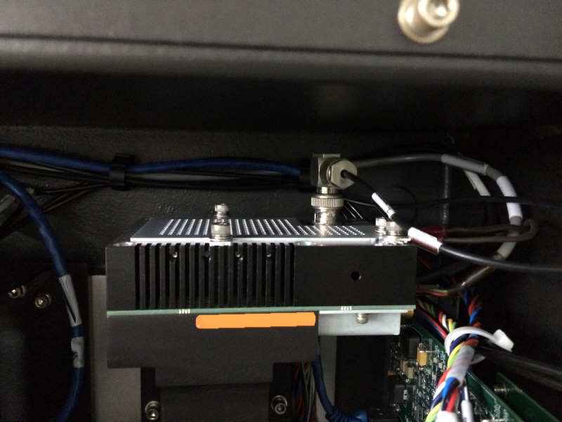
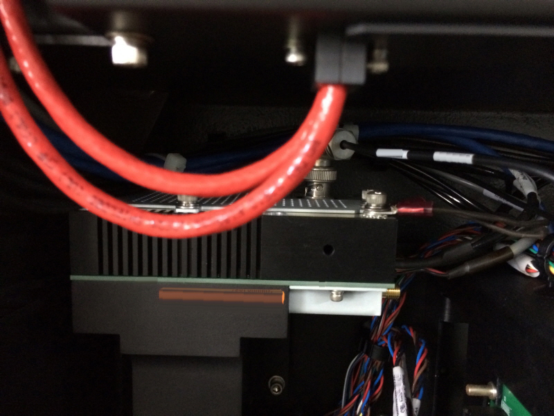
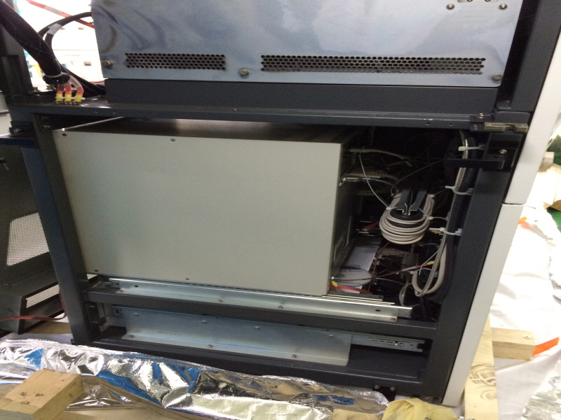
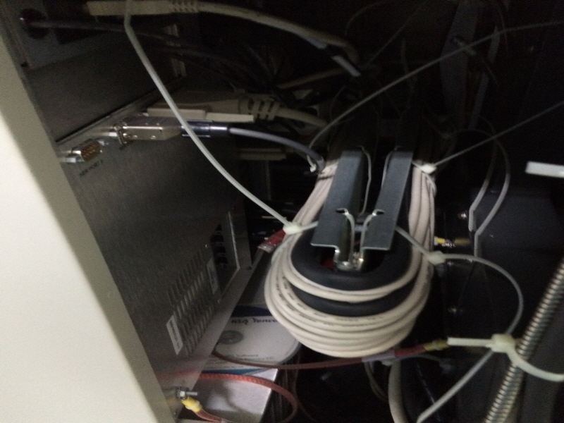
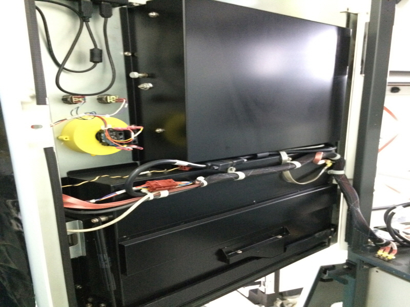
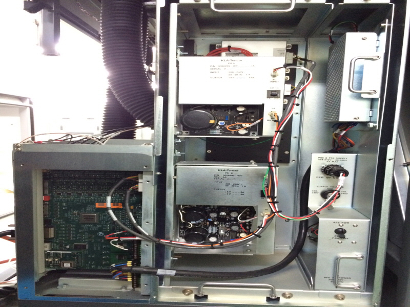
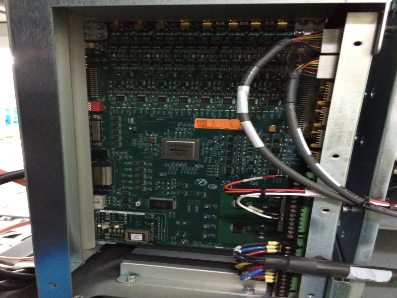
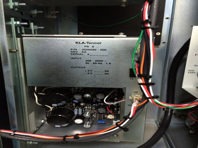
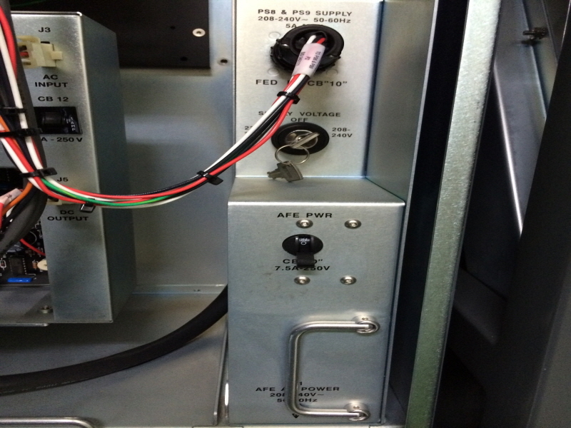
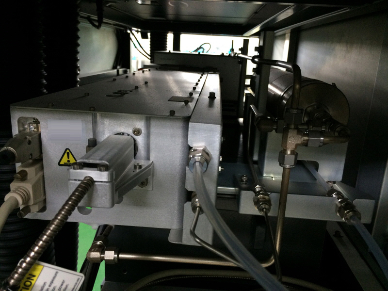
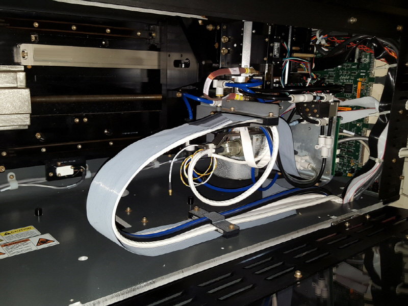
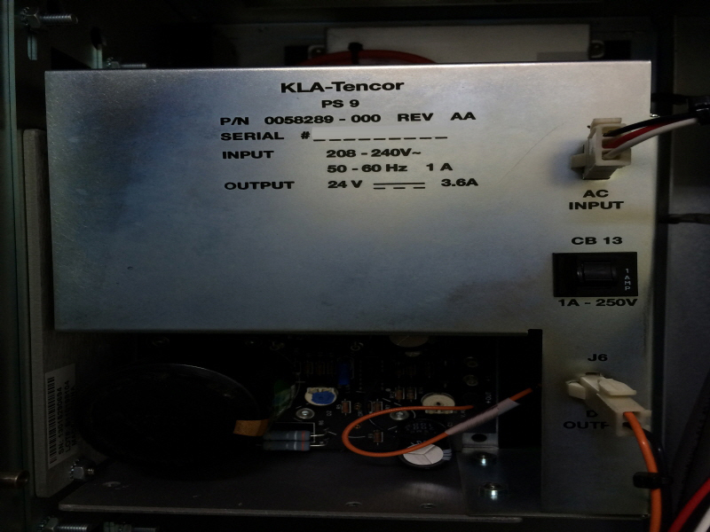
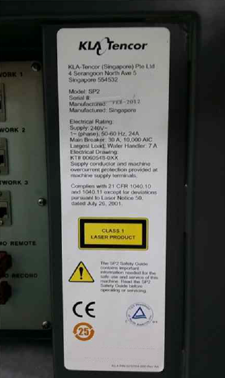
ID: 9099730
Wafer Size: 12"
Vintage: 2012
Inspection system, 12"
Unpatterned Surface Inspection System
Dual FIM/FOUP
Unpatterned Surface Inspection System
Wafer Measurement Module
Optimized sensitivity and Throughput < 37 nm Defect Sensitivity on Polished Bare Silicon
Enables Qualification of Current and Next Generation Substrates, SOI, Strained SOI and Strained Si
Qualification and Monitoring of Process Tools at 90, 65 and 45 nm Technology Nodes
UV Laser Illumination
Defect Map and Histogram with Zoom
iMicroview Measurement Capability
SURFimage
Real-Time Defect Classification (RTDC)
Microsoft XP Operating System
CE Compliant and Certified
Blower Box
Currently powered down and stored in cleanroom
2012 vintage.
KLA / TENCOR SP2 is a mask and wafer inspection equipment designed for the semiconductor manufacturing industry. It is an advanced inspection system that provides high accuracy, fast throughput, and a high degree of flexibility in mask- and wafer-level defect inspection. The unit consists of an imaging subsystem, an analysis subsystem, and a control subsystem, which are interconnected to form a closed-loop inspection machine. The imaging subsystem operates on the principles of digital optics, combining opto-mechanical and digital technologies to acquire images of microstructures on the wafer and mask. The digital optics used in the tool offers superior image resolution and enables the detection of sub-micron defects. The imaging asset consists of an optical head and a detector. A 6-axis robotic positioning model provides imaging of the entire substrate, with the ability to detect and identify defects on layers from the top of the wafer as well as the reverse side. The analysis subsystem is the core of the equipment, and consists of software algorithms that enable automated defect inspection. The algorithms are able to detect defects down to 0.1um in size, and are capable of identifying structural defects, mask defects, and particle defects. The algorithms process the images obtained by the imaging subsystem, and use multiple techniques including signal processing, pattern recognition, analytical modeling, and statistical analysis to identify and classify defects. The control subsystem performs the overall control and synchronization of the imaging and analytical subsystems. This subsystem is responsible for managing the system's task parameters and data flow, such as image acquisition, defect detection, and misalignment correction. The control subsystem also ensures that all functions are carried out in an optimized manner, with fast and accurate analysis of the data. In summary, KLA SP-2 is an advanced mask and wafer assembly inspection unit that provides superior image resolution, high accuracy, and fast throughput. Its powerful imaging and analysis subsystems and the control subsystem combine to create a robust and flexible closed-loop inspection machine that is ideal for the semiconductor manufacturing industry.
There are no reviews yet