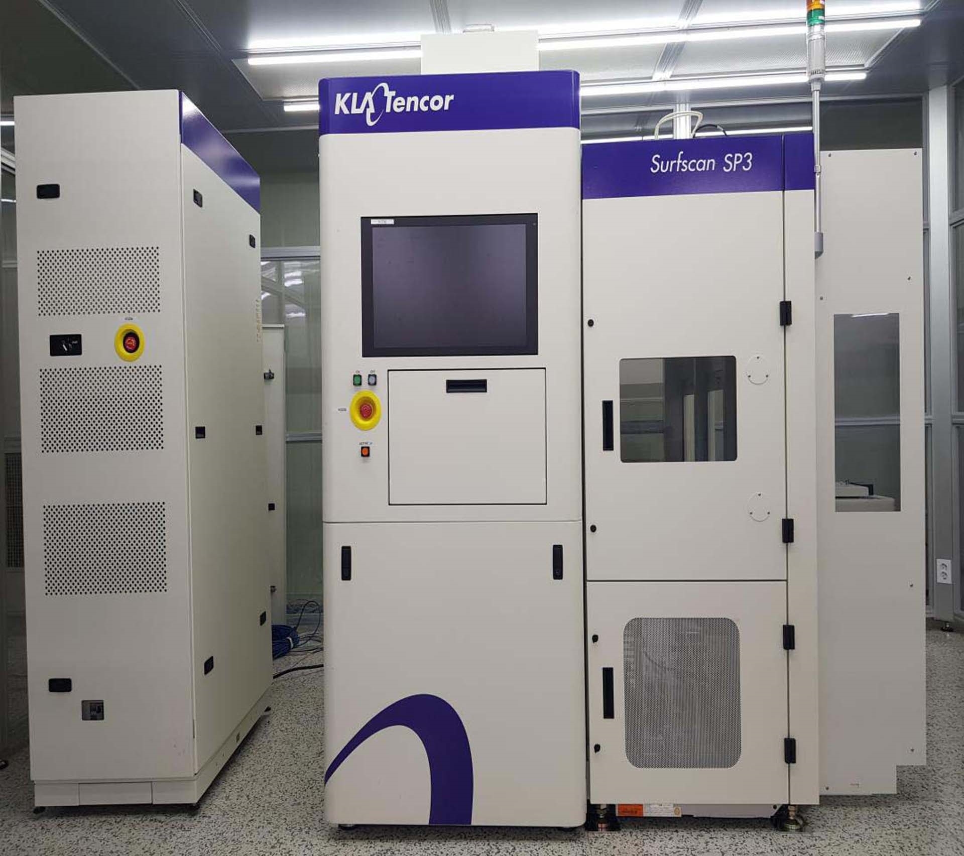
Used KLA / TENCOR SP3 #9235735 for sale
It looks like this item has already been sold. Check similar products below or contact us and our experienced team will find it for you.
Tap to zoom


Sold
ID: 9235735
Wafer Size: 12"
Vintage: 2011
Wafer surface inspection system, 12"
Optimized sensitivity and throughput: ≤ 28 nm Defect sensitivity on polished bare silicon
Sensitivity modes:
Standard throughput inspection mode
High throughput inspection mode
High sensitivity inspection mode
Advanced illumination optics supporting modes:
Normal illumination
Oblique illumination
Inspection station configured for 12" vacuum handling
Equipped with cool white panels
PHOENIX Tri FIMS Vacuum wafer handler, 12"
Laser power modulator
GEM/SECS and HSMS
E84 Enablement for AMHS, TFIMS
(3) OHT HOKUYO PI/O Infrared communication (Hardware) devices
Options:
Advanced SURF monitor analysis capabilities
Bright field (DIC)
XFS Lens:
Tungsten (W)
Copper (Cu)
Poly
2011 vintage.
KLA / TENCOR SP3 is a next-generation mask and wafer inspection equipment, designed to provide advanced defect inspection capabilities for advanced semiconductor fabrication. The system utilizes a combination of light optical microscopy (LOM), scanning electron microscopy (SEM) and computational imaging techniques to provide detailed coverage of the complete mask and wafer pattern, as well as sub-resolution defects. KLA SP-3 unit uses a volumetric 3D imaging method to achieve non-destructive imaging with stunning detail. This is accomplished through the combination of two acquisition techniques: Direct Inspection in which the mask and wafer features are imaged directly as layer-to-layer stacks, and Generative Emulation in which a high-resolution image of the reconstructed feature stacks is generated. In terms of optical capabilities, TENCOR SP 3 provides full-field imaging up to 256mm x 256mm scan regions, with a wide dynamic range and excellent contrast. In addition, advanced image processing capabilities, such as edge-detection and contrast enhancement, are available. For SEM imaging, SP3 is designed to provide extremely high resolution images, with a max resolution of 5nm. This allows for detailed examination of high-resolution mask and wafer features, and for identification of sub-resolution defects that can not be detected by traditional inspection techniques. In addition to providing imaging capabilities, TENCOR SP3 also features automated defect detection algorithms, which allow for the detection of individual defects within a pattern. This allows for rapid screening of defects across the entire mask and wafer patterns, reducing inspection time and allowing greater accuracy. SP 3 machine is capable of performing both manual and automated inspections, and offers a comprehensive package of metrology and defect analysis tools. This allows engineers to quickly and accurately assess the performance of masks and wafers, and to identify and isolate defects. The tool is also designed to be ultra-compact and lightweight, allowing for use in areas with limited space. Overall, KLA / TENCOR SP 3 is an extremely advanced mask and wafer inspection asset, providing unprecedented imaging and defect detection capabilities for advanced semiconductor fabrication. With its high resolution imaging, automated defect detection algorithms, and ultra-compact size, TENCOR SP-3 is an ideal choice for the job.
There are no reviews yet