Used KLA / TENCOR Spectra CD 100 #9399340 for sale
URL successfully copied!
Tap to zoom


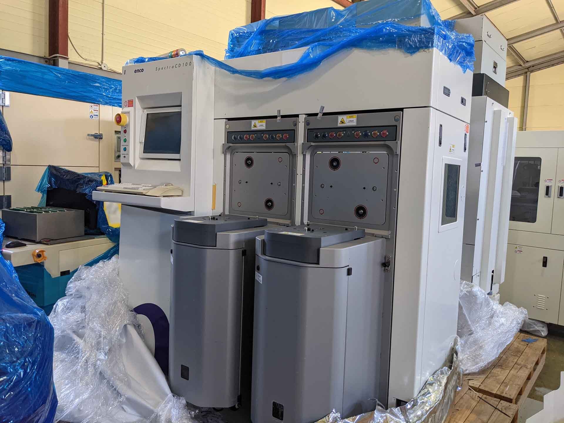

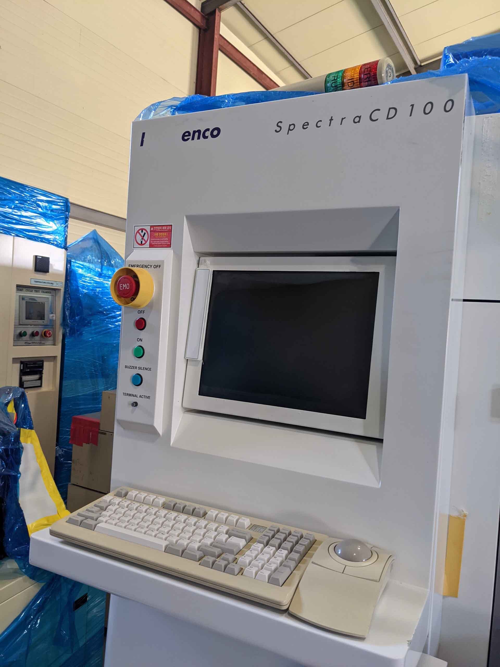

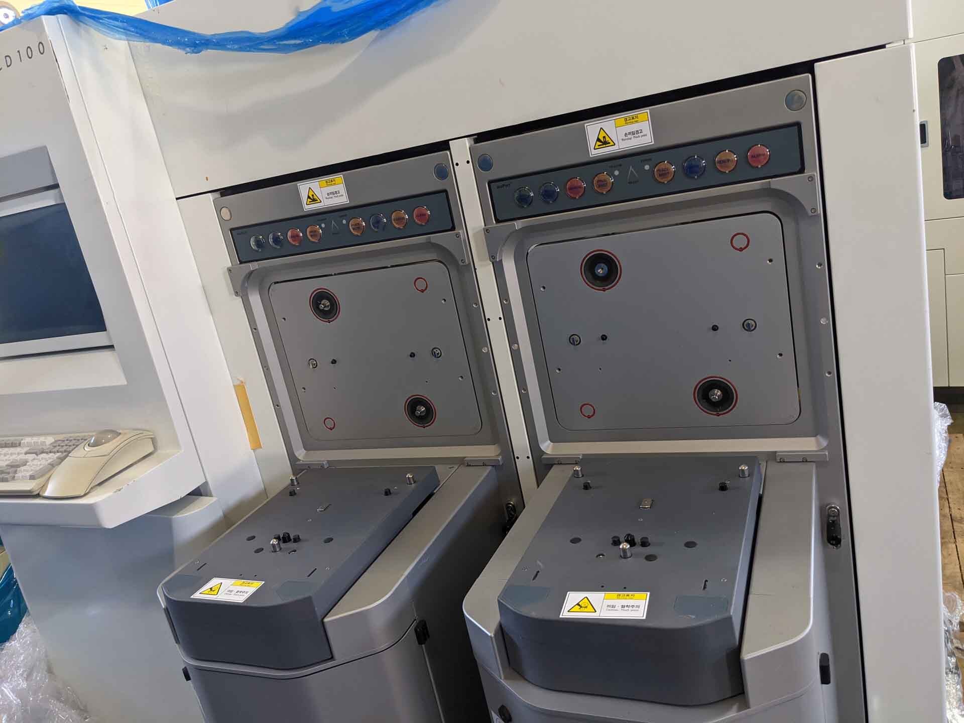


KLA / TENCOR Spectra CD 100 from KLA is a mask and wafer inspection equipment designed to detect microscopic defects and contamination in semiconductor process layers. It uses advanced algorthms to accurately and reliably inspect all aspects of masks, wafers and dielectrics. The system combines sensitive optical and imaging technologies to quickly and precisely identify potential process issues and particle contamination. The integrated detection algorithms provide an accurate classification of detected particles. The unit's optics are highly efficient, and allow for both high-contrast imaging and detection of small defects and low-level contaminations. The application of advanced optical hardware and software leads to faster and higher quality process optimization. KLA Spectra CD 100 is equipped with stage technology that allows for the scanning of large surface areas in a single scan. With its superior degree of translation and rotation accuracy the machine obtains a large number of images from each wafer. The powerful software is equipped with a range of customizable report formats, which allow for customized reporting based on specific applications. The tool can also be configured to detect and analyze a wide range of anomalies and potential defects. The Mask and Wafer Inspection Toolkit (MWIT) features multiple modes, including full-die and spectral imaging. Using spectral imaging, the asset can detect and classify single particles, small dust particles, and spillover, even on larger surfaces. The advanced and easy-to-use software also provides analytic tools for interpreting, visualizing, and organizing measurement data. The software can generate automated reports in both graphical and pdf formats. TENCOR SPECTRACD 100 is ideal for both design and FA applications. With its reliable and accurate performance it is suitable for detecting particle contamination, smearing, and registration issues down to sub-micron and nanometer-level resolution. The advanced optics and imaging capabilities can detect small defects even in areas with weak contrast. This powerful model is quick, reliable and offers users an economical solution for advancing process development and improving mask and wafer inspection capabilities.
There are no reviews yet
