Used KLA / TENCOR Surfscan SP2 #293814035 for sale
URL successfully copied!
Tap to zoom

ID: 293814035
Inspection system
UV laser
Defect map
Real-Time Defect Classification (RTDC)
Operating System: Windows
Advanced Illumination Optics
Powder Coat Painted Panels
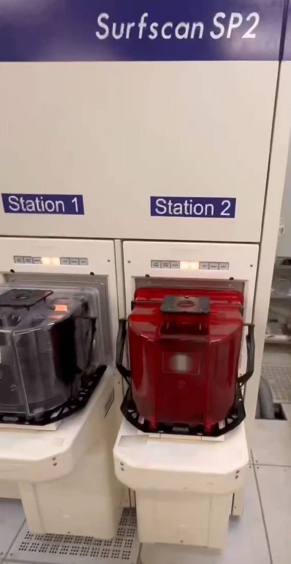
Phoenix Dual FIMS Vacuum Wafer Handler (PP), 12"
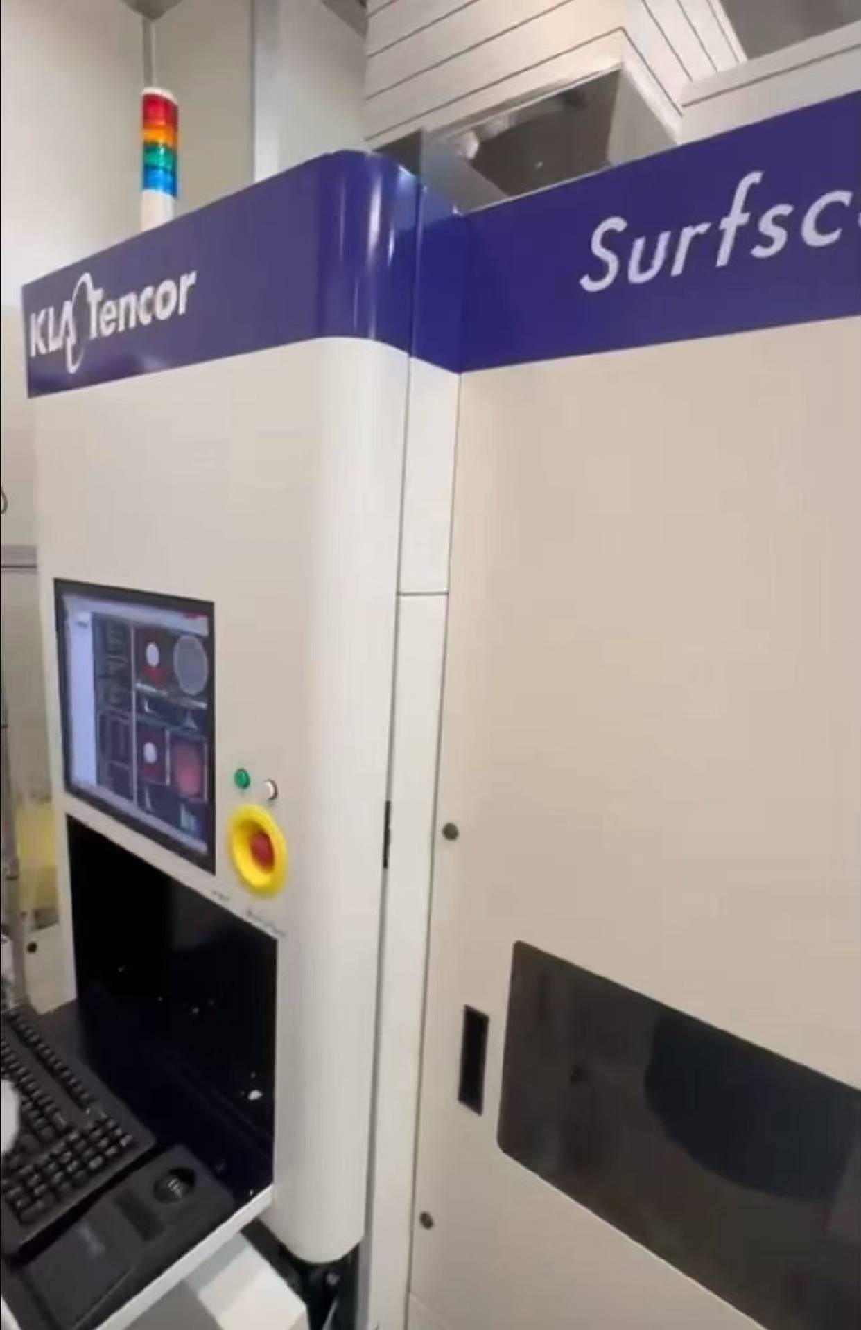
4‑Color Light Tower (RGB)
Ion Shower for Phoenix Dual
XY Calibration Wafer, 12"
Dryer for COE.
KLA / TENCOR Surfscan SP2 is a full field optical critical dimension (CD) SEM based mask and wafer inspection equipment. It is a compact and maintenance-free system developed for the automated inspection of front-end masks and wafers. KLA Surfscan SP2 is equipped with a sophisticated imaging unit, which is able to generate high quality images of even the most complex mask and wafer structures. This machine consists of a monochromated field emission scanning electron microscope (FE-SEM), a cryogenic specimen stage, and a motorized XYZ stage for accurate positioning of the specimen. The FE-SEM operates with a resolution of 0.2nm and can detect structures as small as 4nm. Its integrated automated measurement and analysis software enables the user to access information from individual layers, which helps in the process of assessing the quality of the samples. Moreover, TENCOR SURFSCAN SP 2 provides precise control of the beam current and the cooling tool to protect the samples against damages. Surfscan SP2 also has an intuitive user interface to allow users to quickly and easily set up and start inspecting without having to refer to the manual. Furthermore, the asset also provides reliability and repeatable performance to ensure accuracy of results. In addition, TENCOR Surfscan SP2 offers a fast and reliable process for inspecting the samples. By using the automated focus feedback loop, the model can quickly adjust its focus and get accurate results. The equipment is provided with a wide variety of extensions, which includes defect review, data export, review database management, and process control. KLA SURFSCAN SP 2 is ideal for a wide range of semiconductor applications such as mask inspection, wafer review, circuit layout verification, lithography simulation, overlay analysis, process control, and failure analysis. It supports different technologies like PDK, BiCMOS, and DRAM and can be used to inspect multiple layers of structures. The system is capable of integrating AutoAdjust, which is a powerful rule-based tool used for automated feature measurements and defect reporting. Moreover, it can also be used for defect classification and wafer metrology. Overall, SURFSCAN SP 2 is a reliable and efficient mask and wafer inspection unit that is able to perform the most complex analysis. Its advanced features and capabilities make it the ideal choice for all semiconductor industries.
There are no reviews yet