Used LEICA INS 3000 #293689181 for sale
URL successfully copied!
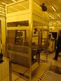
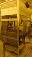
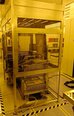
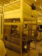
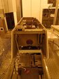
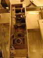
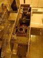
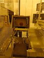
Tap to zoom
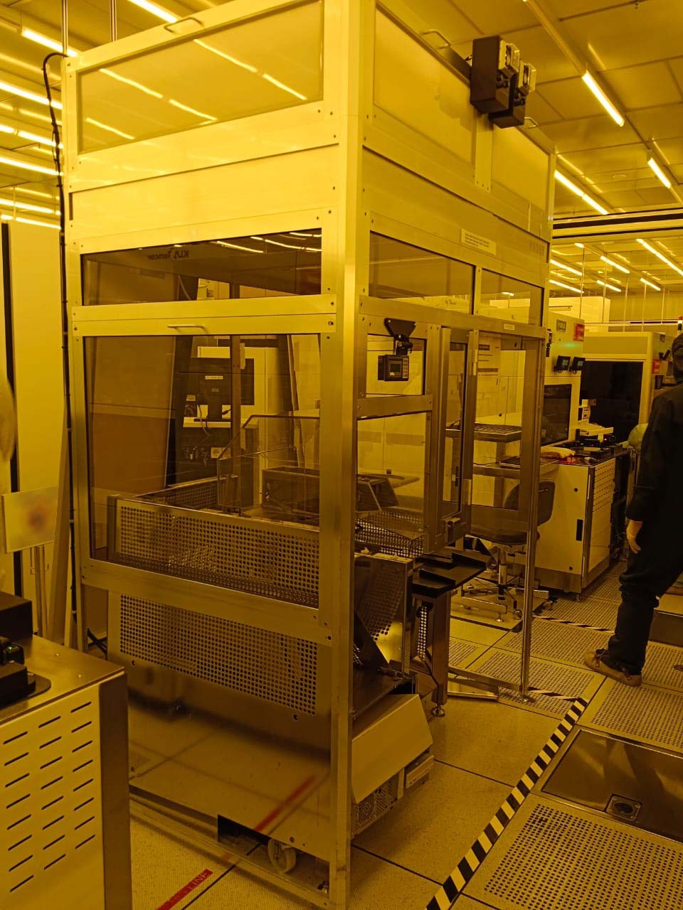

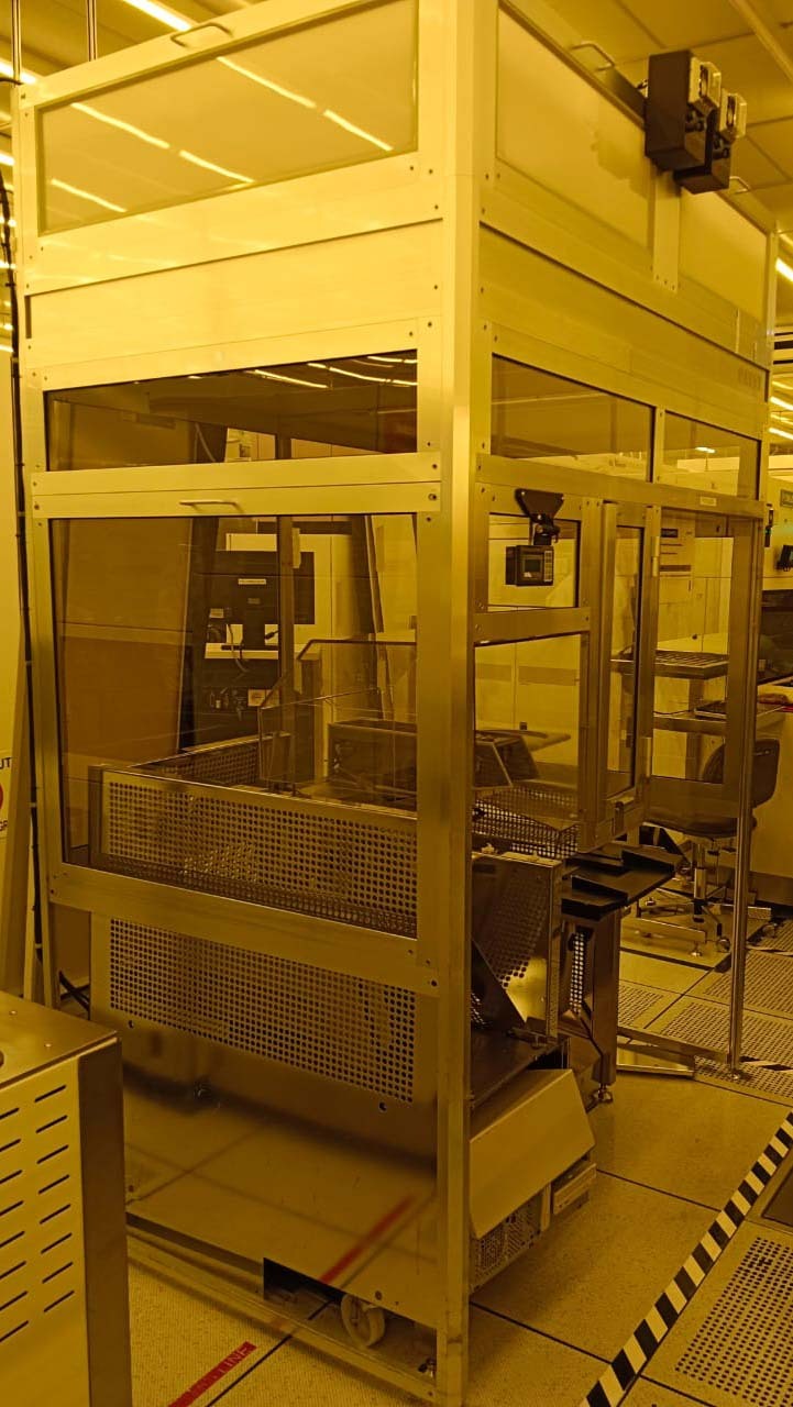
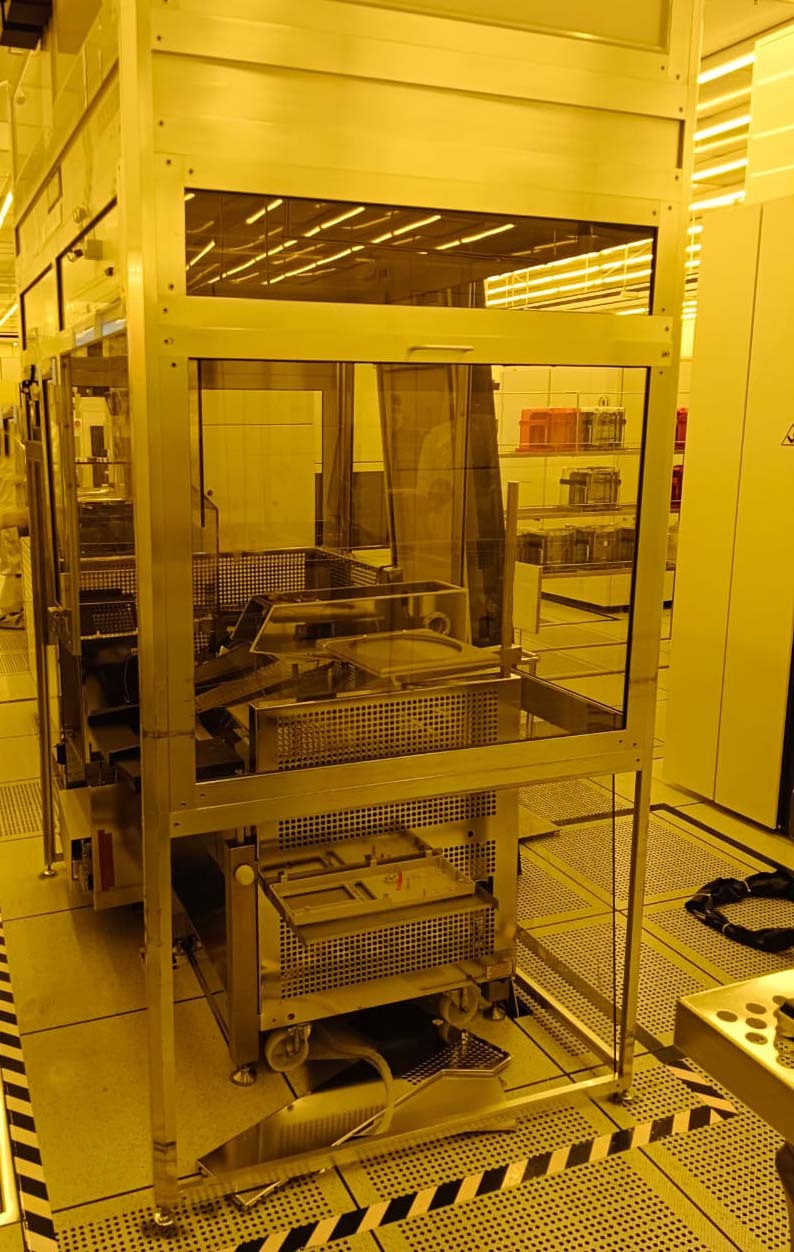
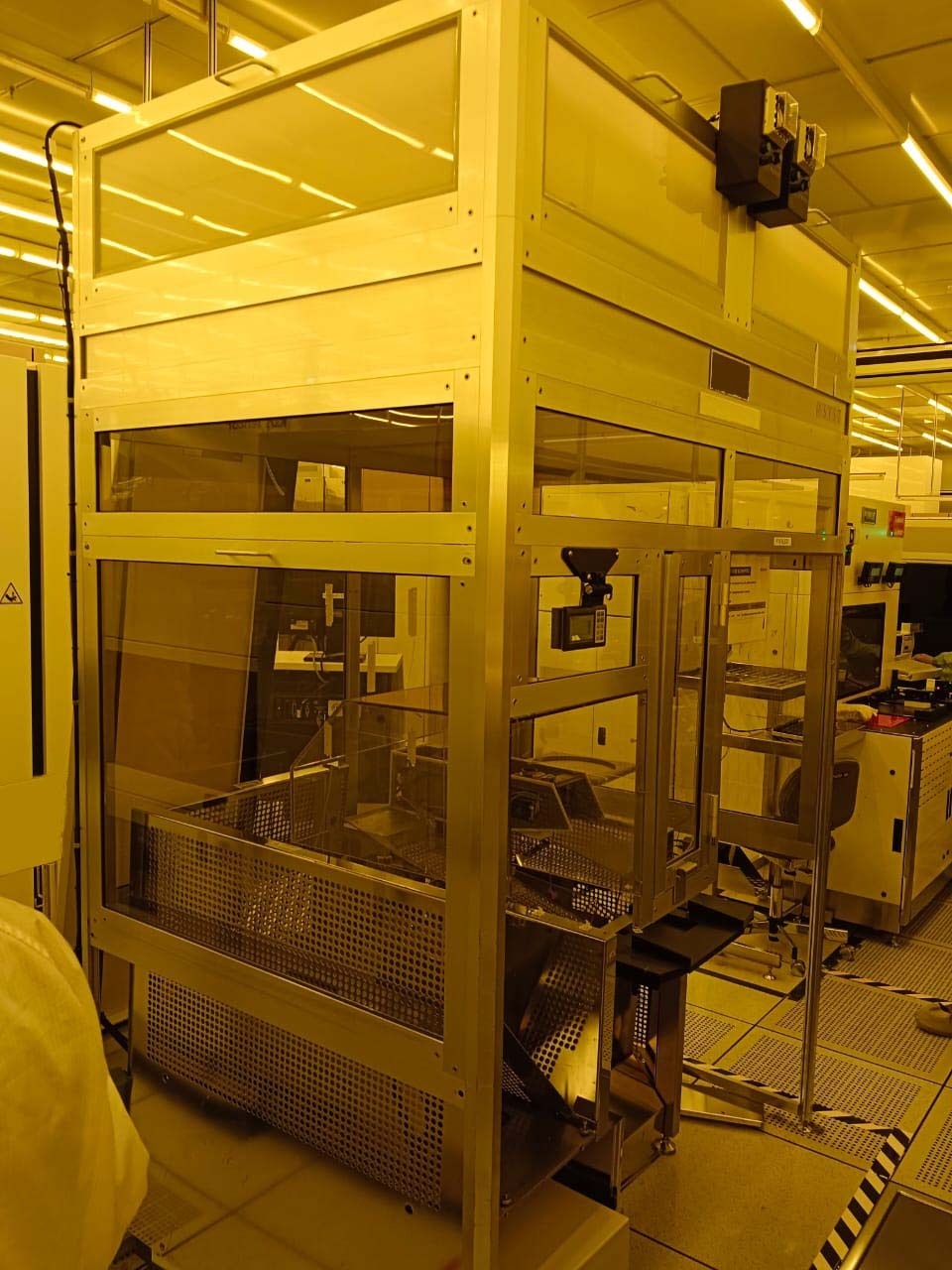
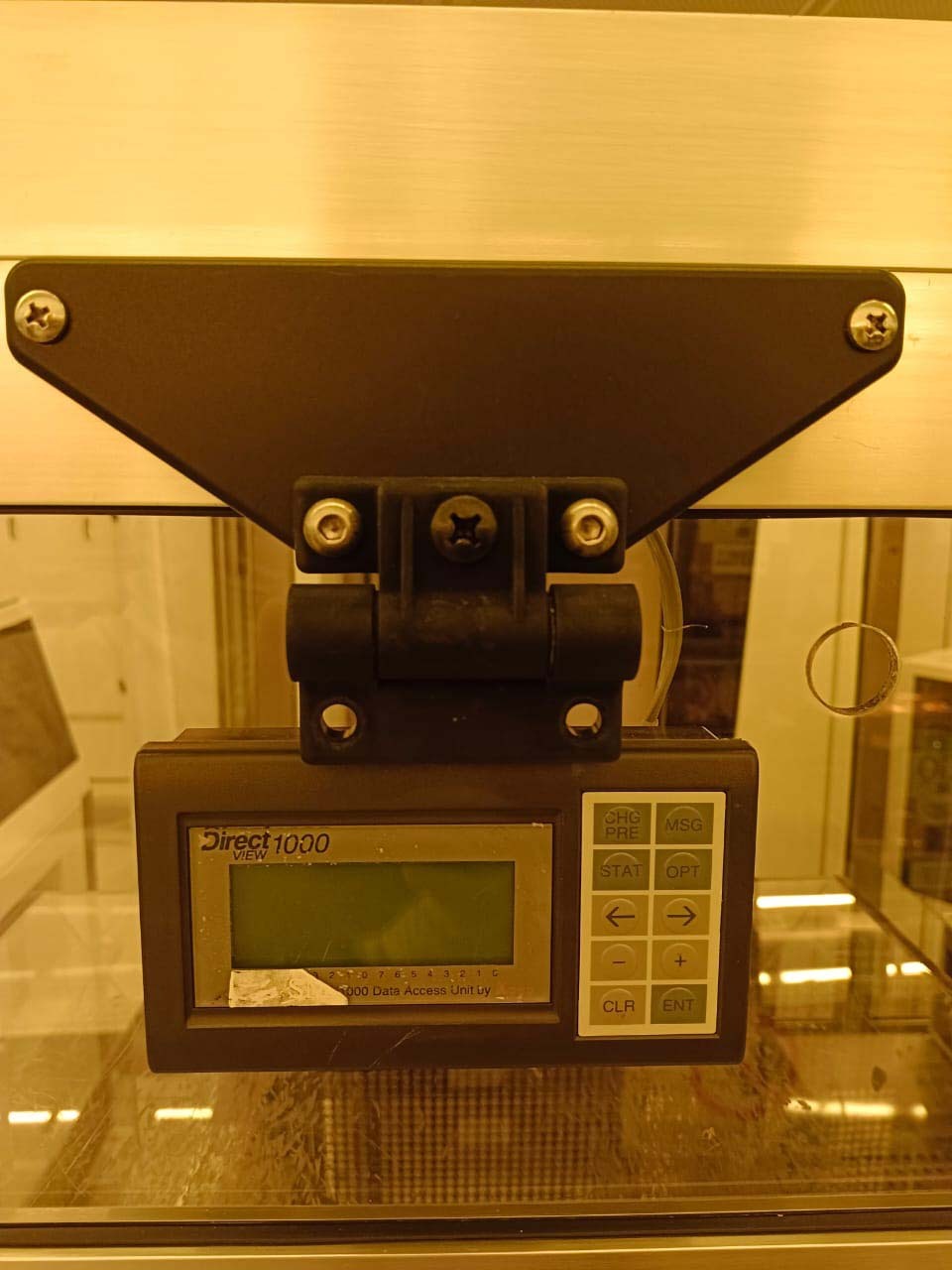
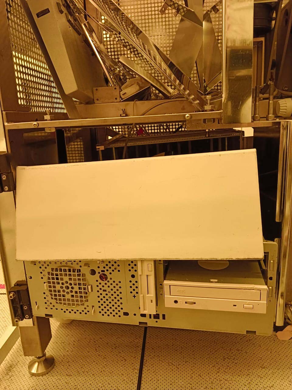
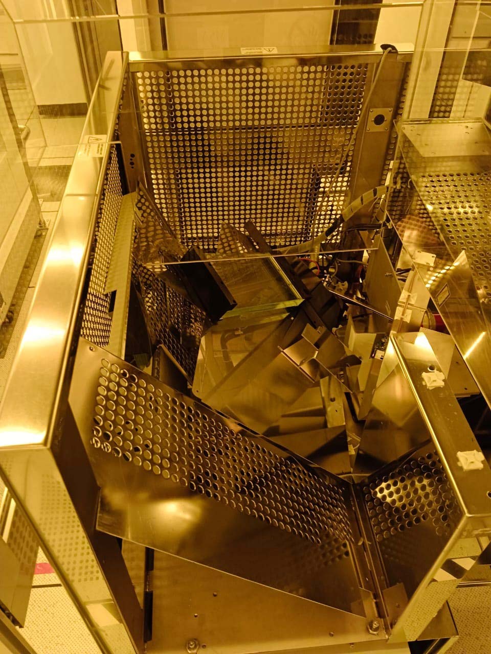
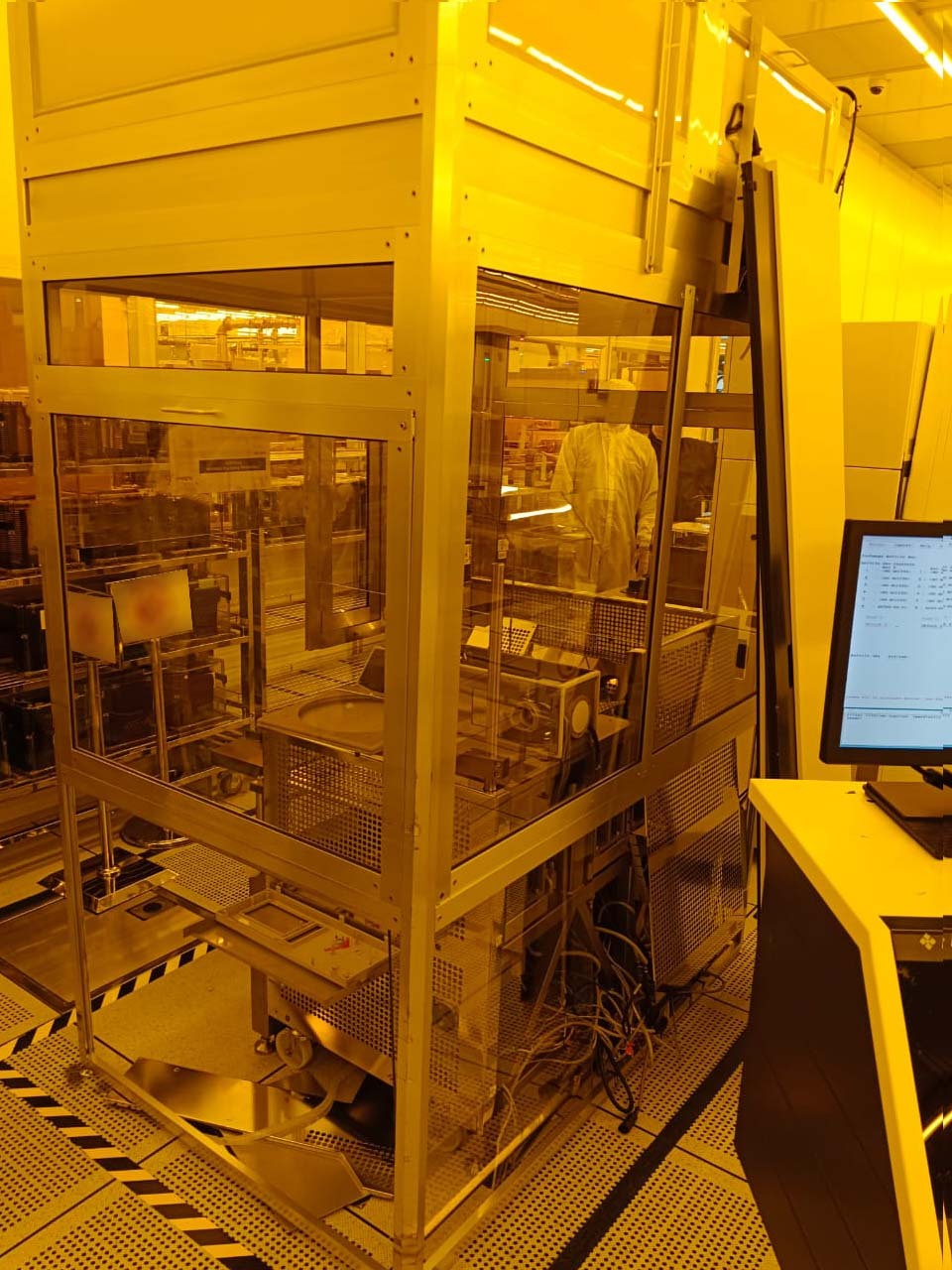
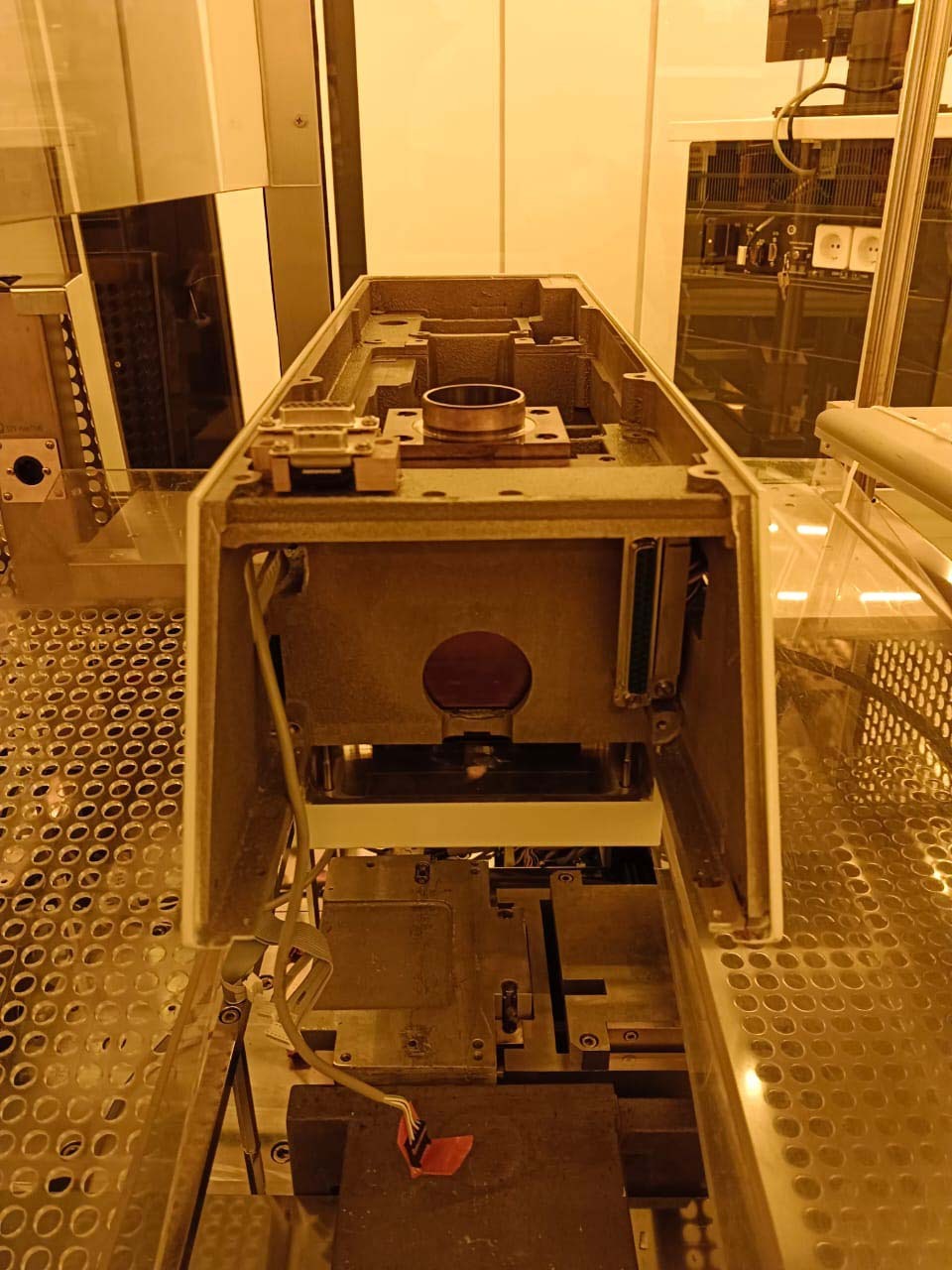
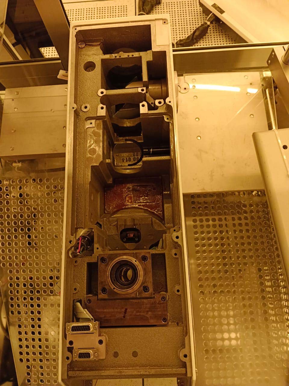
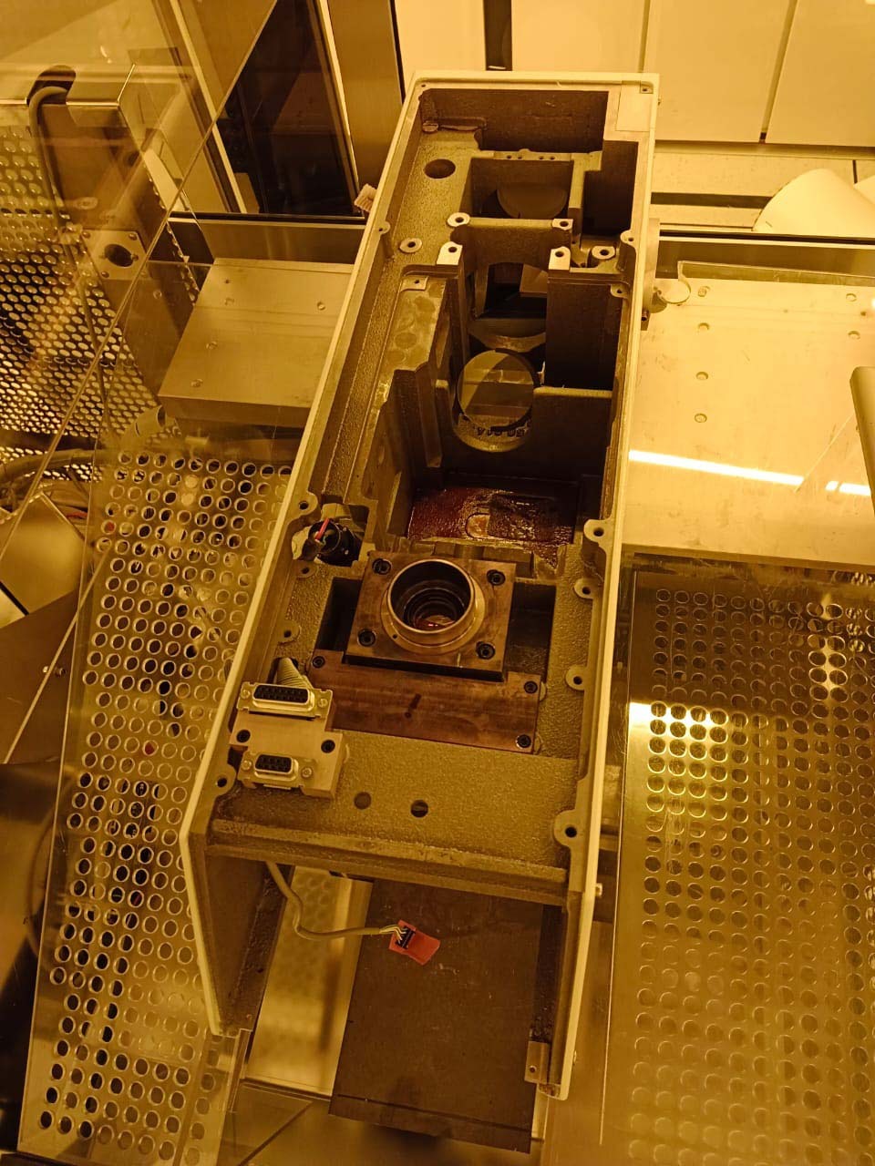
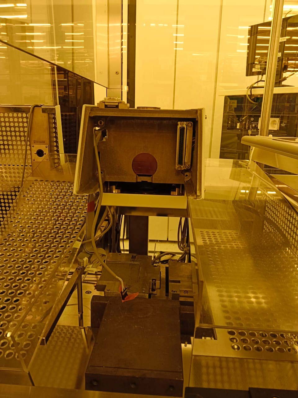
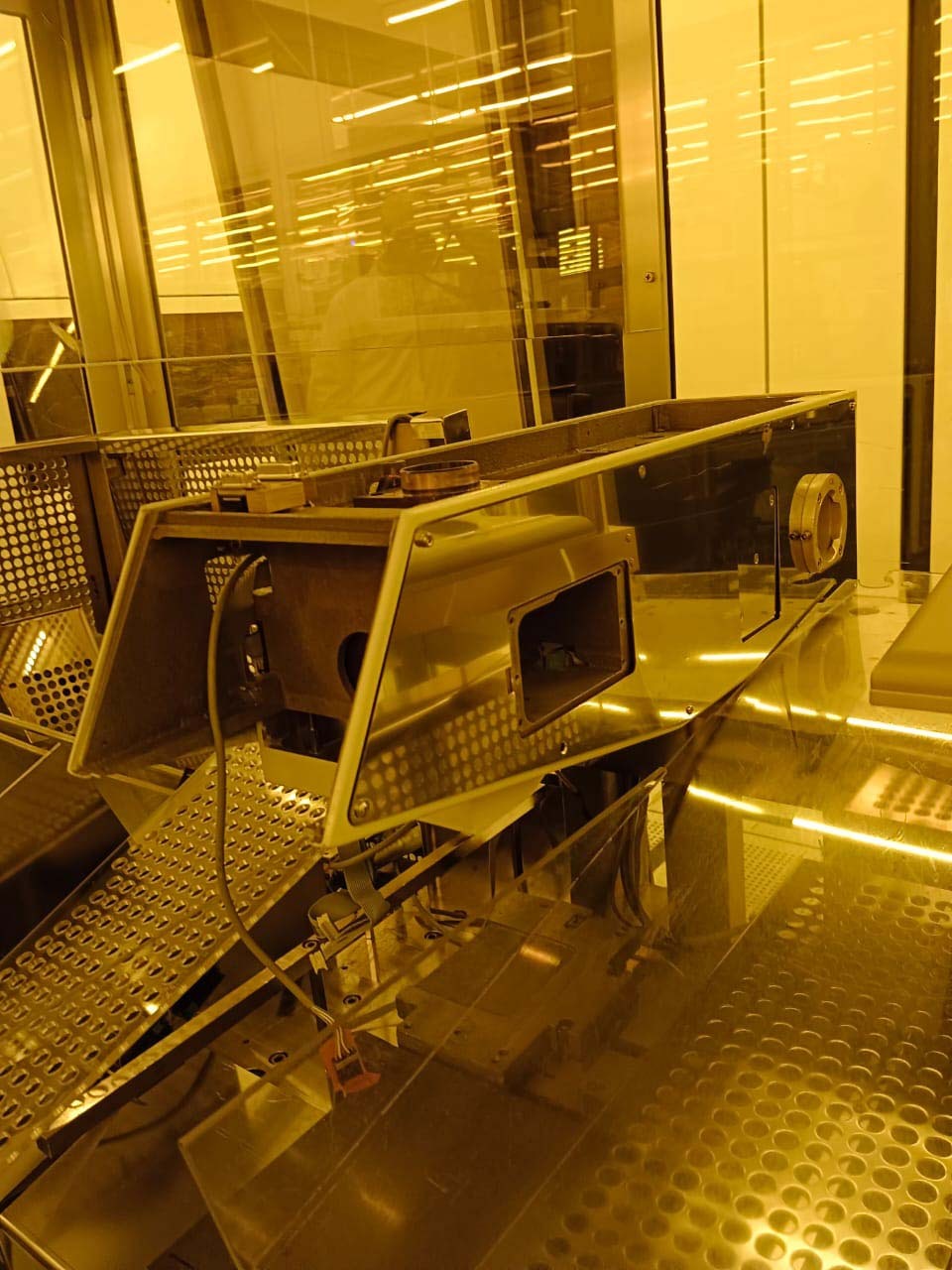
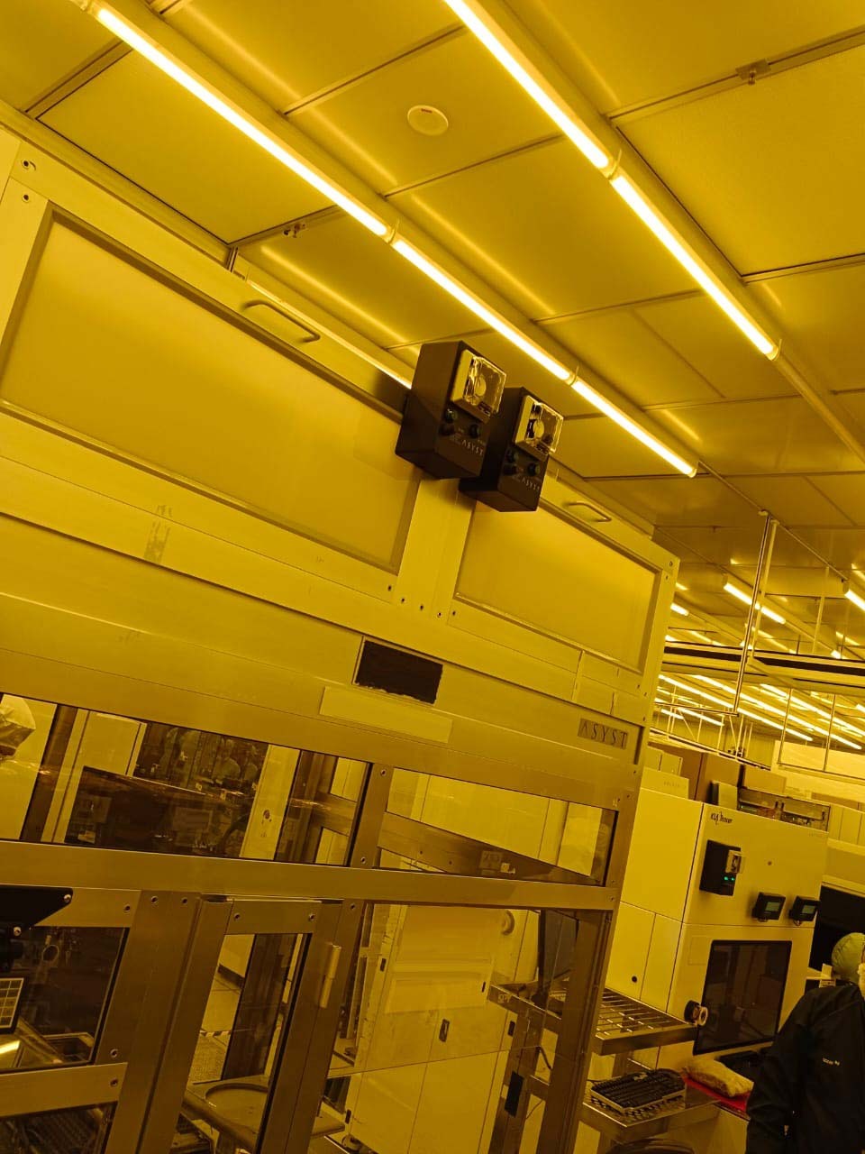
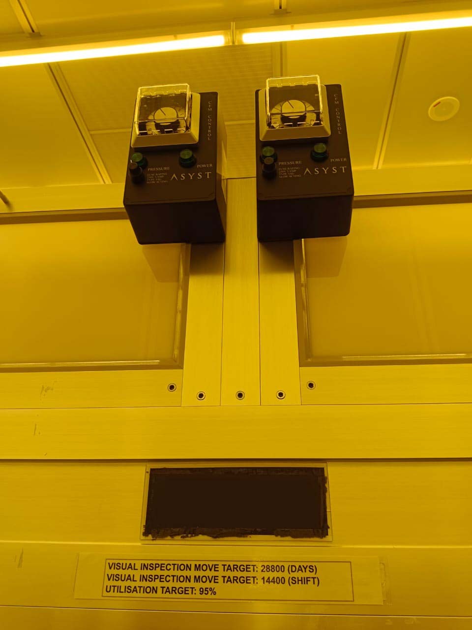
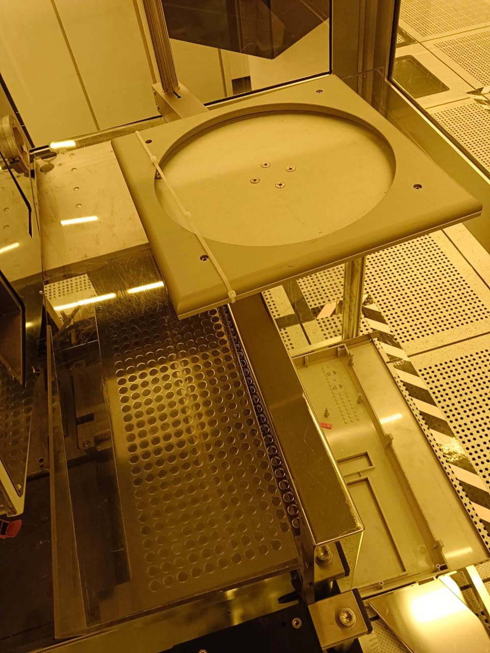
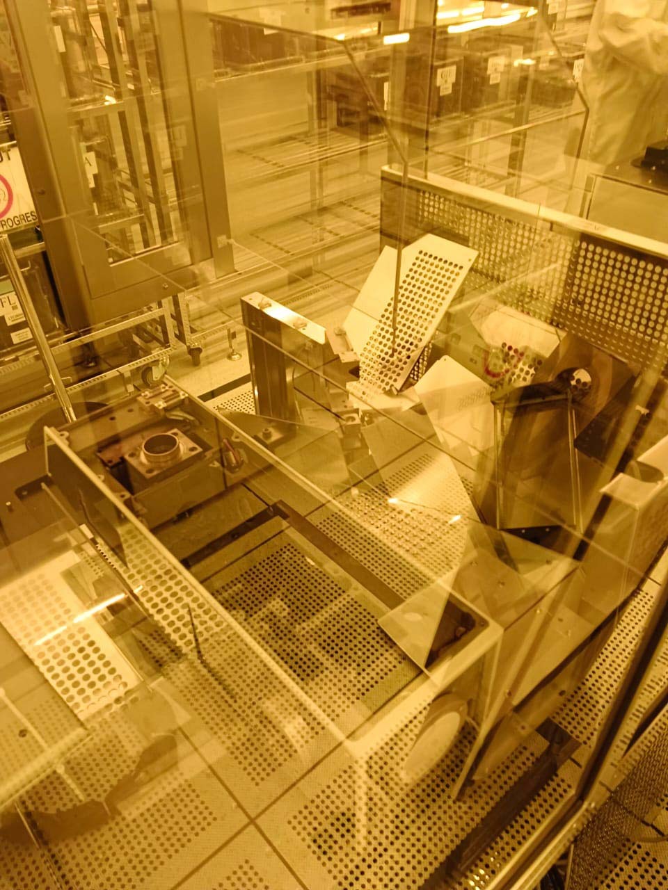
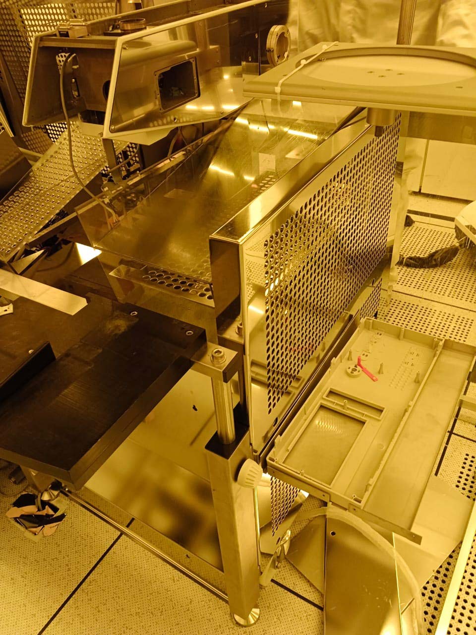
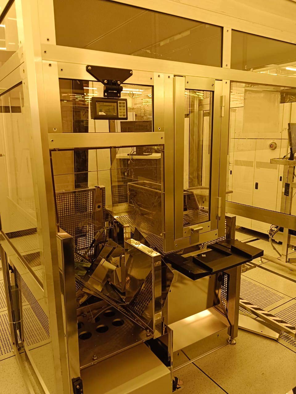
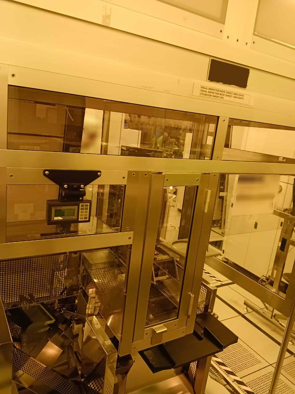
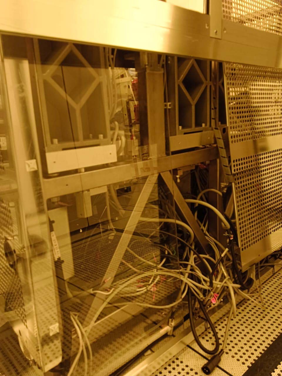
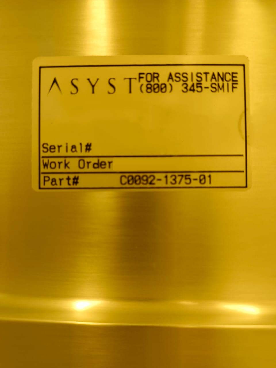
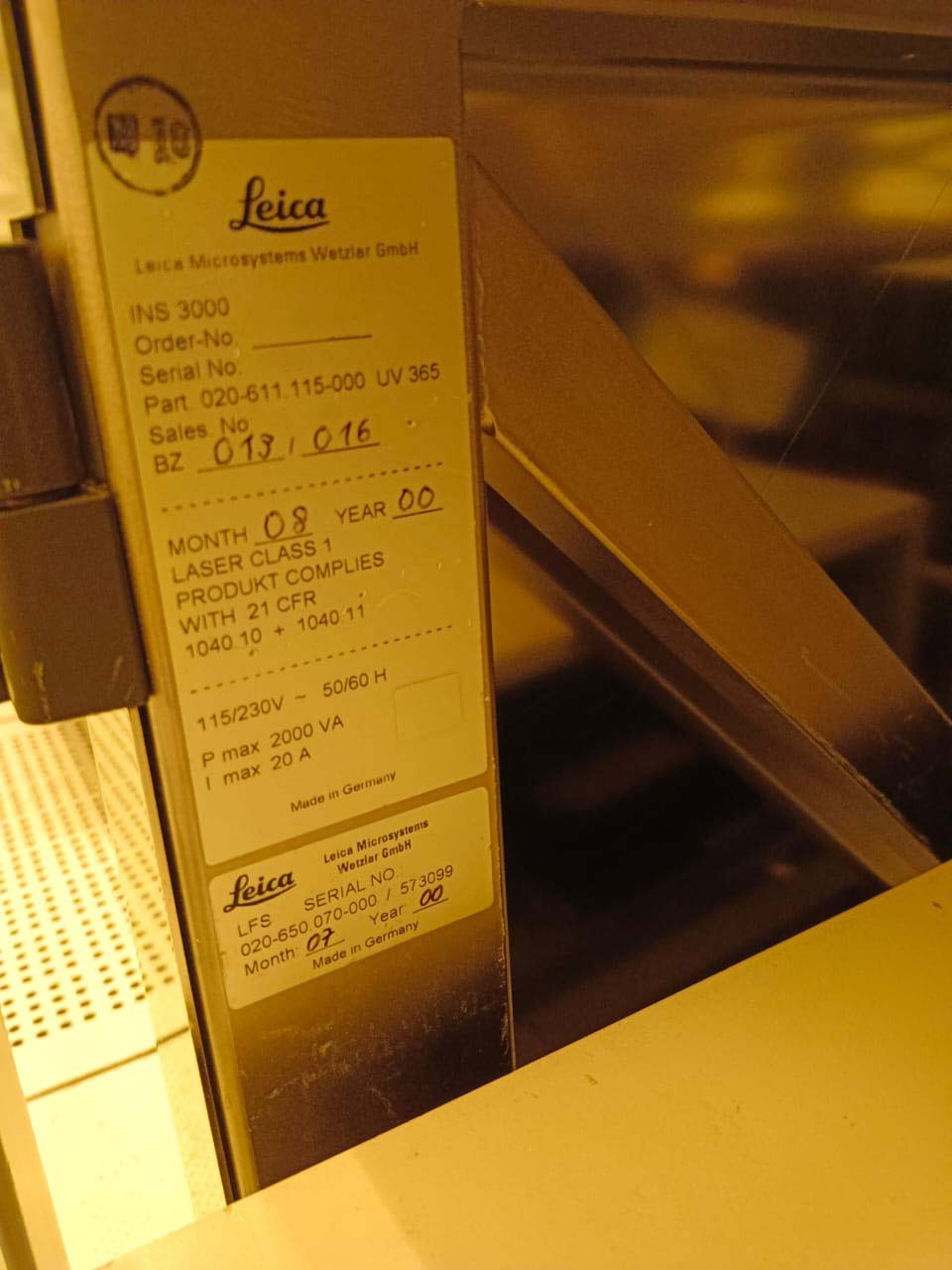
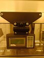
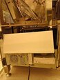
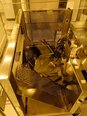
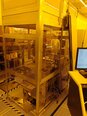
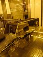
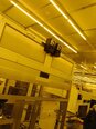
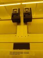
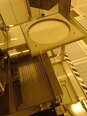
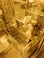
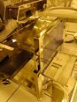
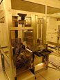
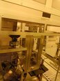
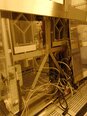
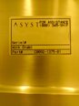
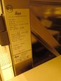
LEICA INS 3000 is a robust mask and wafer inspection equipment recognised for its advanced design, leading resolution, and reliable automated processes. Capable of scanning defect capture of fully automated handling processes up to 300mm wafers, it offers an easy-to use design ideal for separating defects at the most minute level with maximum accuracy. The system operates by detecting, characterising, and sorting defects — both physical and electrical — with its integrated suite of high-resolution optical tools. These include a Tomo Broadband illumination array, a field emission SEM unit, as well as high-resolution RGB imaging. Further benefitting the performance of LEICA INS-3000 is its support for a range of yield-enhancing image processing functions. These include advanced feature and density detection, intelligent pattern recognition, and precision stitching to capture gratings and features down to 0.2μm in size. Furthermore, an integrated defect pre-sorting module offers the highest accuracy levels with existing library data and automated reporting capabilities. This unit is also delivered with numerous flexible analytical tools, mainly to aid engineers in their development of innovative process inspection solutions. The integrated software suite, which features enhanced AutoFE-SAM analysis, includes image illumination control, as well as an improved set of comparative image processing tools. The improved pattern recognition capabilities are complemented with on-site training sessions and tutorials that allow customers to customise their visual inspection analysis. Thanks to its flexible configuration, INS 3000 machine also supports a variety of production operations such as end-face and wire bond inspections, particle inspection, and a multitude of applications specific inspections. Its tight integration with other automated equipment guarantees faster and more reliable processing performance. Altogether, INS-3000 tool offers a reliable automated mask and wafer inspection. It is designed to meet the growing demands of the semiconductor industry for a tool with advanced detection capabilities, fast throughput, and high-grade defect sorting features.
There are no reviews yet