Used LEICA / VISTEC IMS 2000 #9283662 for sale
URL successfully copied!
Tap to zoom


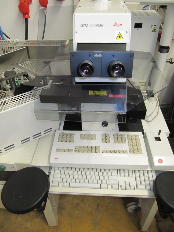

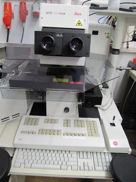

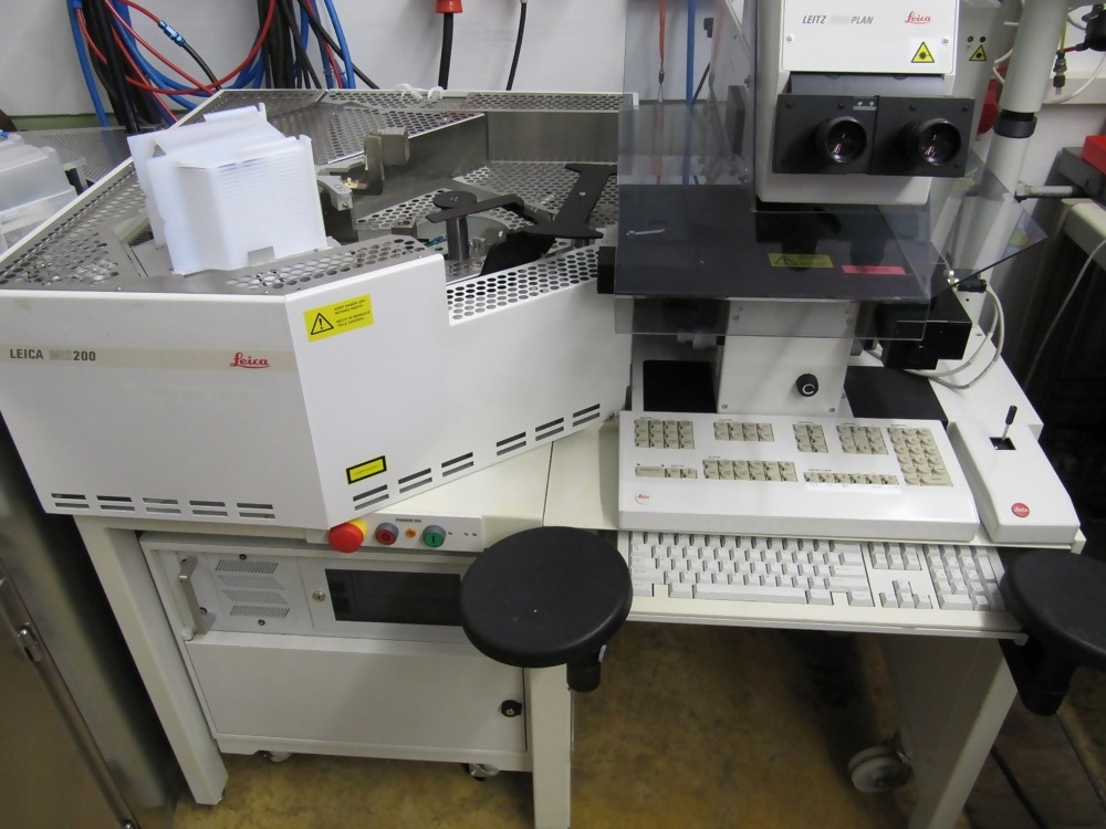


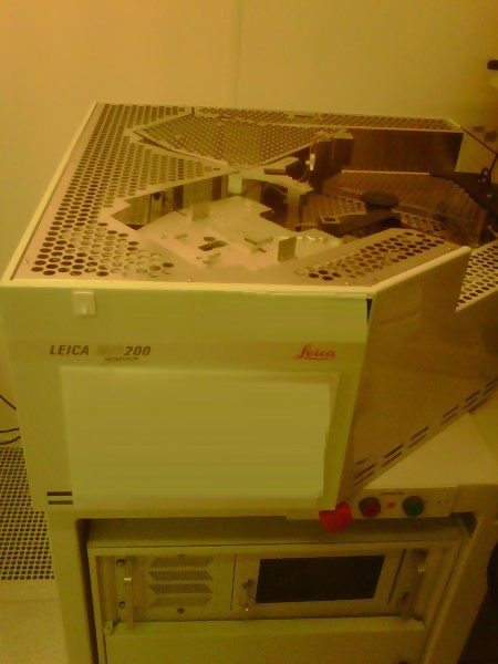


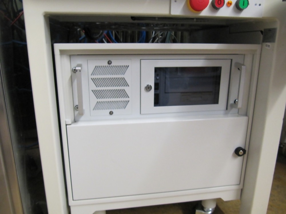

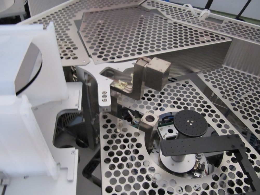


ID: 9283662
Wafer Size: 8"
Wafer inspection system, 8"
Cassette to cassette
Wafer handling
LEICA ERGOPLAN microscope with motorized X/Y 225 mm movement table
Leica PL Fluotar 10X, 20X
Leica PL APO 50X, 100X, 150X
Ergonomic Binocular viewing optics with Leica L plan 10X /25 eyepieces
ICR option (Interference Contrast Reflection (Nomarski Princible))
Laser autofocus
Integrated Dual Secondary Magnification with 1X, 1.6X and 2.5X range
Photographic Eye Tube with zoom adapter lense with 0.55X - 1.1X magnification range
Lamphouse
power supply: 100W, 12V
Halogen bulb
Donpisha 3CCD color vision camera module
Sony CMA-D2 camera adapter
Sony HR Trinitron
Model: PVM-1453MD monitor
HP Super VGA
Model: D2 HeNe laser
SMC digital pressure sensor
Power: 120V / 230V, 50 Hz / 60 Hz
CE marked.
LEICA / VISTEC IMS 2000 is a mask and wafer inspection equipment designed to perform a complete evaluation of the geometry and topography of structures in semiconductor fabrication processes. It features high-resolution imaging capabilities and the ability to detect both surface defects as small as 1 micro metre, as well as mask artefacts. Its advanced software capabilities enable both optical measurement and automated process control, with a wide range of measurement options available. The system is particularly suitable for detecting defects in areas of dense circuitry, such as dynamic random access memory (DRAM) and logic chips. The unit is composed of three main components: an image acquisition machine, a microscope stage, and a control unit. The image acquisition tool comprises a charge-coupled device (CCD) camera and a microscope objective lens. It allows for high-resolution imaging of structures down to the nanometre scale. The microscope stage consists of an X-Y-Z linear stepping mechanism, which provides an accurate and repeatable surface-scanning path for defect detection. It is also capable of automated sample and specimen loading and unloading. Finally, the control asset contains all the necessary image processing and automation capabilities, allowing the user to easily and quickly configure the instrument according to their needs. LEICA IMS 2000 is capable of producing both high-resolution digital images of wafer and masks, and post-processing of these images for defect detection and measurement. The imaging model is equipped with "smart filter" technology, which allows for the automated detection of both surface defects and mask artefacts. The microscope stage, meanwhile, is capable of a flat-field topography measurement, with an accuracy down to 1 nanometre. Additionally, the microscope can be programmed with complex grids and patterns for automated defect detection and wafer registration. VISTEC IMS 2000 is designed to offer a reliable inspection performance, with a complete analysis delivered in a short time frame. This makes it an ideal choice for quality assurance and process control in advanced semiconductor fabrication applications. Its intuitive software interface and reliable, automated features help to simplify several tedious and lengthy tasks, which can help to improve production efficiency.
There are no reviews yet


