Used LEICA / VISTEC INS 1000 #9265472 for sale
URL successfully copied!
Tap to zoom
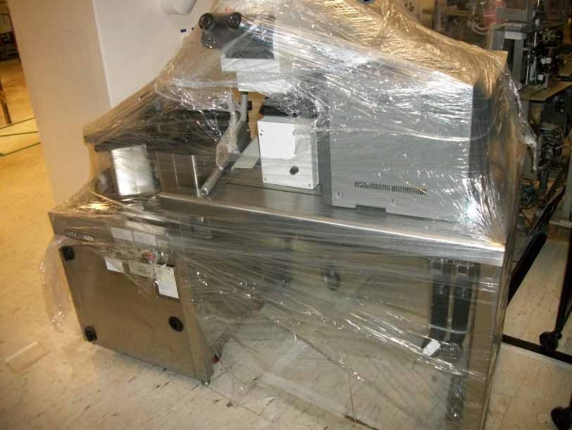

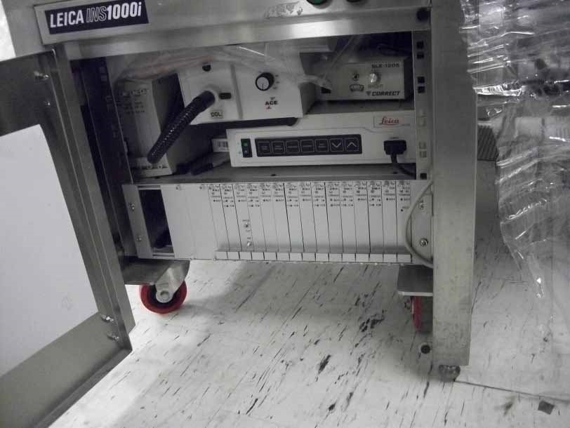

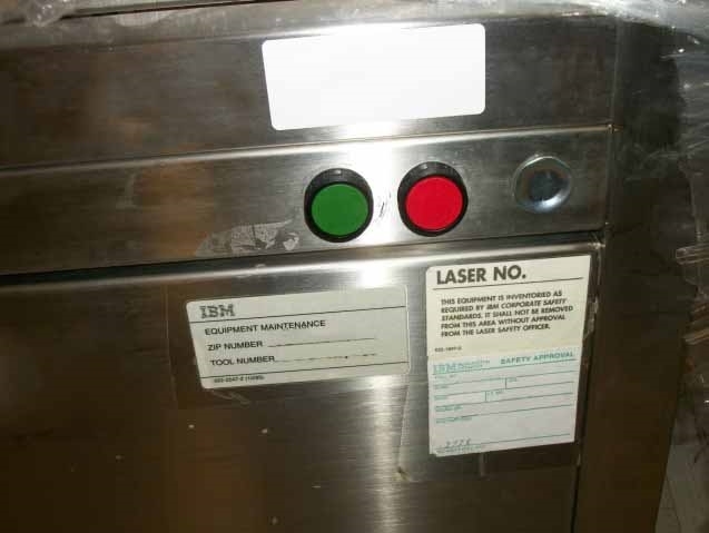

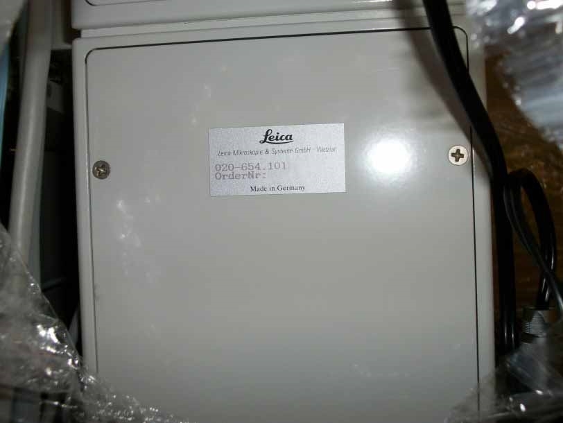

LEICA / VISTEC INS 1000 is a platform for mask and wafer inspection. It is a fully automated equipment for the accurate determination of defects and process aberrations. The system is capable of identifying and quantifying defects down to the nanometer level. It offers excellent image analysis capabilities and is ideal for applications in research, development and manufacturing. LEICA INS 1000 is a multi-channel optical inspection unit that uses a combination of scanning electron microscopy and optical microscopy to inspect the quality of masks and wafers. The machine comes with a built-in laser alignment tool, integrated high-resolution camera, and a fully automated software and hardware suite that provides reliable and repeatable results. The asset can analyze both etched and un-etched surfaces. The model has both manual and automated modes of operation, allowing it to be used in both research and production environments. The manual mode provides the accuracy and capabilities necessary for research while the automated mode is designed to be used in larger sample inspection projects. The equipment has been designed to be highly adaptable and can be used in a wide range of applications. The integrated software has been designed to provide users with a comprehensive set of tools for analyzing and quantifying defects and process aberrations. The software supports the extraction, comparison and presentation of defect data for both masks and wafers. The software also includes a suite of data presentation modules for producing custom graphics, graphical overlays, and defect maps. The system also includes a number of optional accessories such as automated image analysis software and analysis libraries, sample transfer systems and a variety of sample holders for accommodating different sizes and configurations of sample materials. This allows users to customize their setup to suit their particular needs. VISTEC INS1000 offers the ability to analyze up to four wafers at a time and offers an image resolution of 3 nanometers. This makes it ideal for applications requiring the highest image quality, such as semiconductor device manufacturing. The unit is designed to be easy to use, ensuring that even inexperienced users can obtain reliable and accurate results. The machine is highly reliable, with a low-maintenance design and robust construction. It is also exceptionally compact, enabling it to be integrated into existing processes. This makes it an excellent choice for semiconductor production, as well as research and development.
There are no reviews yet

