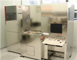
Used LEICA / VISTEC LDS 3300M #180137 for sale
It looks like this item has already been sold. Check similar products below or contact us and our experienced team will find it for you.
Tap to zoom


Sold
ID: 180137
Wafer Size: 4" - 8"
Vintage: 2002
Automated Macro and Micro Defect Detection & Classification, 4" - 8"
(2) Loadports Open Cassette
SW Version VISCON NT ADD5.0.1.5581 SP1-F2
SW-Options: Inspection, EBR, Spot Check, Programmed Inspection, Review, Bare Wafer Alignment, KLA Image, Grab, Service Tools; Wafer-ID Reader Siemens-OCR
HSMS Interface
Microscop Options: Objectivs: 2,5x, 5x, 10x, 20x, 50x, 100x
Brightfield and Darkfield illumination
LFS/Z-Autofocus
Stage position repeatability < 2µm
MIC System Controller: Windows NT4
LAN Macro Options: Brightfield and Darkfield illumination (flash)
Sensitivity >30µm (Surface defects), >50µm (Embedded defects)
Capture rate > 95%; Repeatability > 90%
Macro ADC
MAC System Controller: Windows NT4; Dual CPU Pentium 3 2,8GHz
RAID Storage
LAN BR Options: Darkfield illumination
Accuracy < 100µm
2002 vintage.
LEICA / VISTEC LDS 3300M is an advanced mask and wafer inspection equipment designed for the semiconductor industry. It incorporates the industry leading LEICA 3D automated microscopy technology, enabling high-resolution defect detection even during complex 3D optical inspection.This system provides full wafer visualization with true metrology capabilities, ensuring fast and accurate results with no manual intervention. LEICA LDS3300M is capable of detecting and analyzing specific structural defects, pattern distortions and contaminate particles on masks and wafers. It uses pattern recognition capabilities to detect subtle shape or size differences in the patterns and reconstruct a 3-dimensional image based on high-resolution optical inspection data. The 3D images can then be evaluated and inspected at the nanometer level. The unit is equipped with a high-precision wafer stage and a proprietary image-processing software, allowing users to easily and quickly detect small defects from complex mask and wafer patterns. The advanced optical design of the machine also ensures maximum resolution and dynamic range in a wide variety of lighting conditions. VISTEC LDS 3300 M offers a wide range of inspection capabilities, including scanning at a variety of fields of view, scan sizes, and multiple pattern depths. Other features include automated auto-focusing and auto-exposure modes, multi-layer defect review and statistical analysis of results. Advanced image processing algorithms provide instant access to defect results and measure analysis data. The tool also supports image analysis in multiple different formats and can be used in conjunction with optical probing tools. LDS 3300 M asset is designed with operator safety in mind and user-friendly in operation. It is suitable for the most demanding semiconductor fabrication environments and is easy to install, operate, and maintain. The model offers high throughput capability for high device counts and fast sampling speed for quick analysis. These features, combined with its reliable performance, make it an ideal tool for semiconductor mask and wafer inspection.
There are no reviews yet