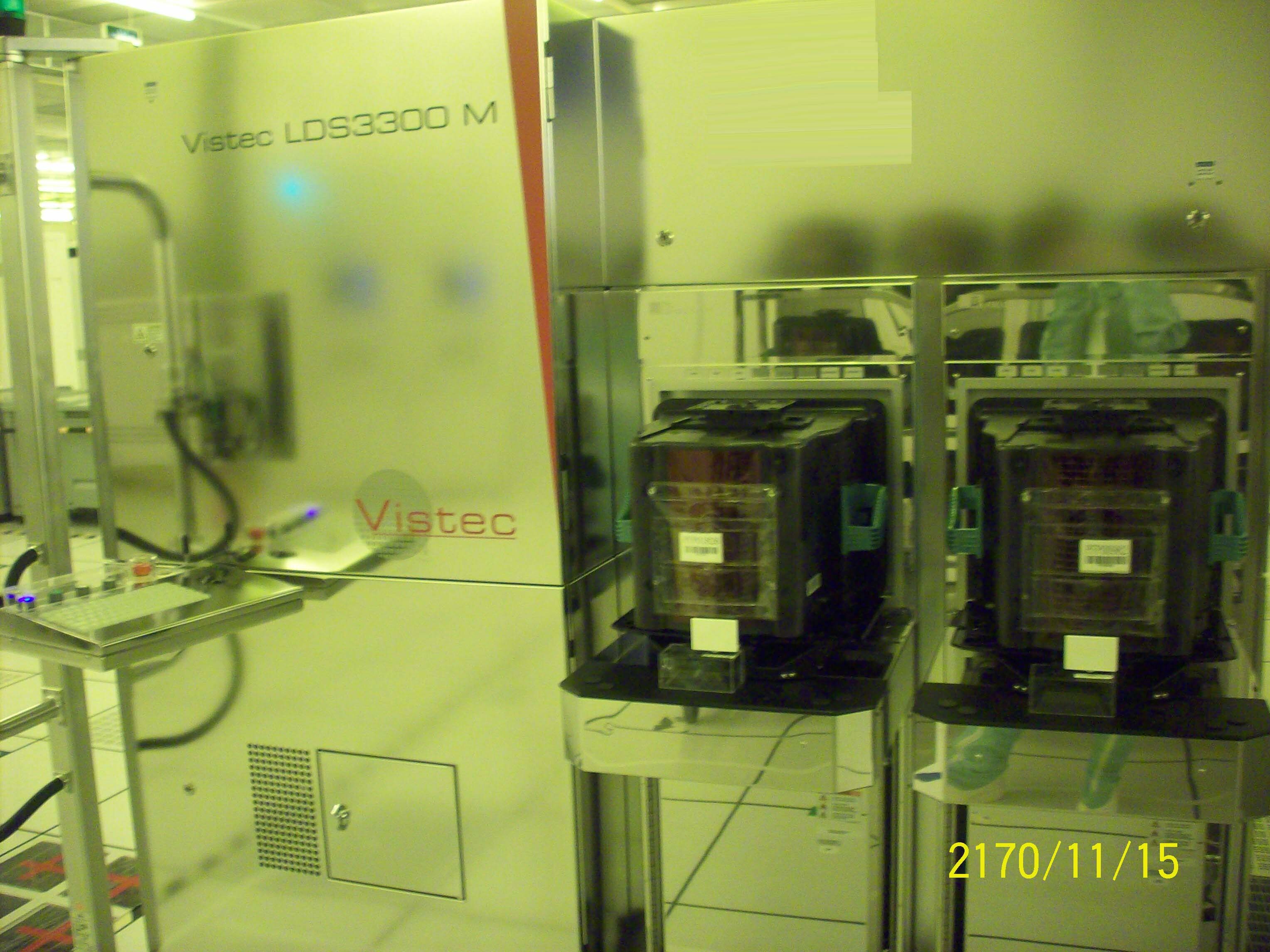
Used LEICA / VISTEC LDS 3300M #9059146 for sale
It looks like this item has already been sold. Check similar products below or contact us and our experienced team will find it for you.
Tap to zoom


Sold
ID: 9059146
Vintage: 2007
Automated macro-defect inspection system
Includes:
Macro inspection
Auto-alignment: Die-based, wafer-based
Defect library
Pixel detection
Alignment control
Color shift and histogram deviation
Global color detection
ROI Editor
Loader module:
(2) Cassette system in SMIF or open cassette version
Wafer existence sensor
Cross slot detection
Contact-free pre-alignment
Macro module:
High precision integrated X/Y Stage
Brightfield/Darkfield/Advanced darkfield illumination system
Illumination high speed strobe
Inspection area of dies, including partial dies
Macro ADC
Optical components
BF and DF imaging
LDS System operation
Image capturing
Specifications:
Throughput, 12": Full die, full wafer, 130 wph
Recipe creation and maintenance: Fast and easy recipe creation and maintenance (<20 min)
Worldwide fab application experience
Edge/bevel inspection
Backside inspection with color imaging
Chip-free area/partial die inspection and review
Process Control:
High resolution spotcheck (Reticle ID check, fuse inspection, overlay check)
Litho alignment mark verification (lower contrast layer inspection capability)
EBR width and shift measurement
Parallel inspection and review
Defocus detection
(3) Load ports options to maximize tool utilization
Parallel process job execution
Full wafer color imaging
Merged trench defect inspection for DRAM
Advanced algorithms:
Tunable sensitivity from wafer center to wafer edge (low false count)
Color defect detection algorithm (low false count)
Global wafer detect detection
Currently installed
2007 vintage.
LEICA / VISTEC LDS 3300M mask and wafer inspection equipment is a fully automated for defect detection and measurement of photo masks and semiconductor wafers. The system consists of two main components -an opto-mechanical parts and a software module. The opto-mechanical parts are constructed with LEICA proprietary immersion optics. This provides the unit with bright and uniform illumination and high-resolution imaging. The machine's optical features include telecentric factory-calibrated lenses, automatic re-focusing, image capturing, and a configurable chromatic aberration compensation. The tool also includes a high-accuracy 4-axis stage with anti-collision technology. This allows alignment and inspection of large-format wafers or oblong stacked multi-level masters with high precision and repeatability. The software module includes a physics-based image processing engine to detect and measure pattern-specific defects. It also provides a comprehensive set of inspection algorithms for various photomask and wafer defects, such as those related to bridge, connecting point, corner, line/space, missing pattern, and pattern displacement. The asset's automated defect analysis processes are highly accurate and enable production engineers to perform timed measurements on samples that traditionally require tedious manual inspection. For full automation, the model's configurable alert thresholds eliminate the need of human supervision and provide real-time feedback to the manufacturing floor. The equipment's comprehensive inspection capabilities have made it an ideal choice for semiconductor wafer and mask production processes. Its non-contact, non-destructive inspection eliminates potential damage to the substrate and is also cost-effective. LEICA LDS3300M has a user-friendly interface that allows users to make quick operations with minimal effort. It also provides detailed defect inspection reports that can be used for quick decisions on future production issues.
There are no reviews yet