Used LEICA / VISTEC LWS 2000 #9115819 for sale
URL successfully copied!
Tap to zoom


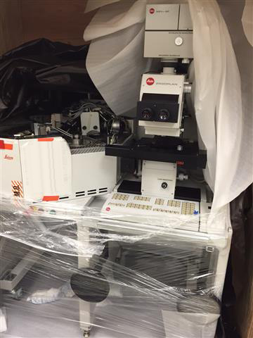
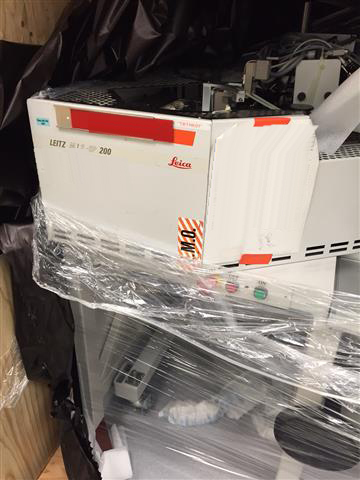
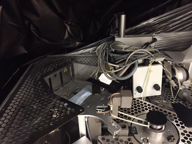
LEICA / VISTEC LWS 2000 Mask & Wafer Inspection equipment is a versatile, high-performance instrument designed for accurate inspection of any photomask or wafer. The system features an automated mask aligner (AMat) with a precise 500mm x 500mm stage and a high-resolution, low-distortion camera to ensure high-quality imaging. LEICA LWS 2000 also features a high-end scan head capable of capturing a large field of view in a single frame. The integrated optics unit has been optimized to precisely align the wafer/mask during imaging, ensuring accurate measurements. The on-board alignment software enables users to establish and adjust focus quickly and accurately. The Mask & Wafer Inspection machine includes an intuitive graphical user interface that enables users to easily access a range of powerful algorithms to analyze acquired images. The integrated metrology tools can be used to evaluate the lithography process, detect any defects such as pattern-edge or pattern-crossing errors, and accurately estimate the critical dimensions of patterns. Advanced stitching and automated qualification tools enable users to rapidly evaluate a range of parameters that may required for wafer qualification. The tool is also capable of detecting color, defects, particles, anomalies, foreign materials, and other variables. It is equipped with a fully configurable set of integrated illumination options that allow for reliable defect detection in arbitrary geometries and features. Furthermore, the asset leverages a range of integrated algorithms to provide rapid defect detection and reporting. Its lightning-fast imaging capabilities enable users to analyze large-scale wafer areas quickly and efficiently. In addition, VISTEC LWS 2000 offers a powerful set of math-oriented tools that can be used to precisely analyze wafer features, identify defects, and measure certain parameters. Users can perform these measurements in absolute, relative, or mixed mode, enabling further analysis and improvement. Furthermore, integrated pattern recognition algorithms are capable of detecting anomalies in complex design structures. This model is ideal for any application that requires accurate wafer measurement and defect detection.
There are no reviews yet


