Used LEICA / VISTEC MIS 200 #9234197 for sale
URL successfully copied!
Tap to zoom
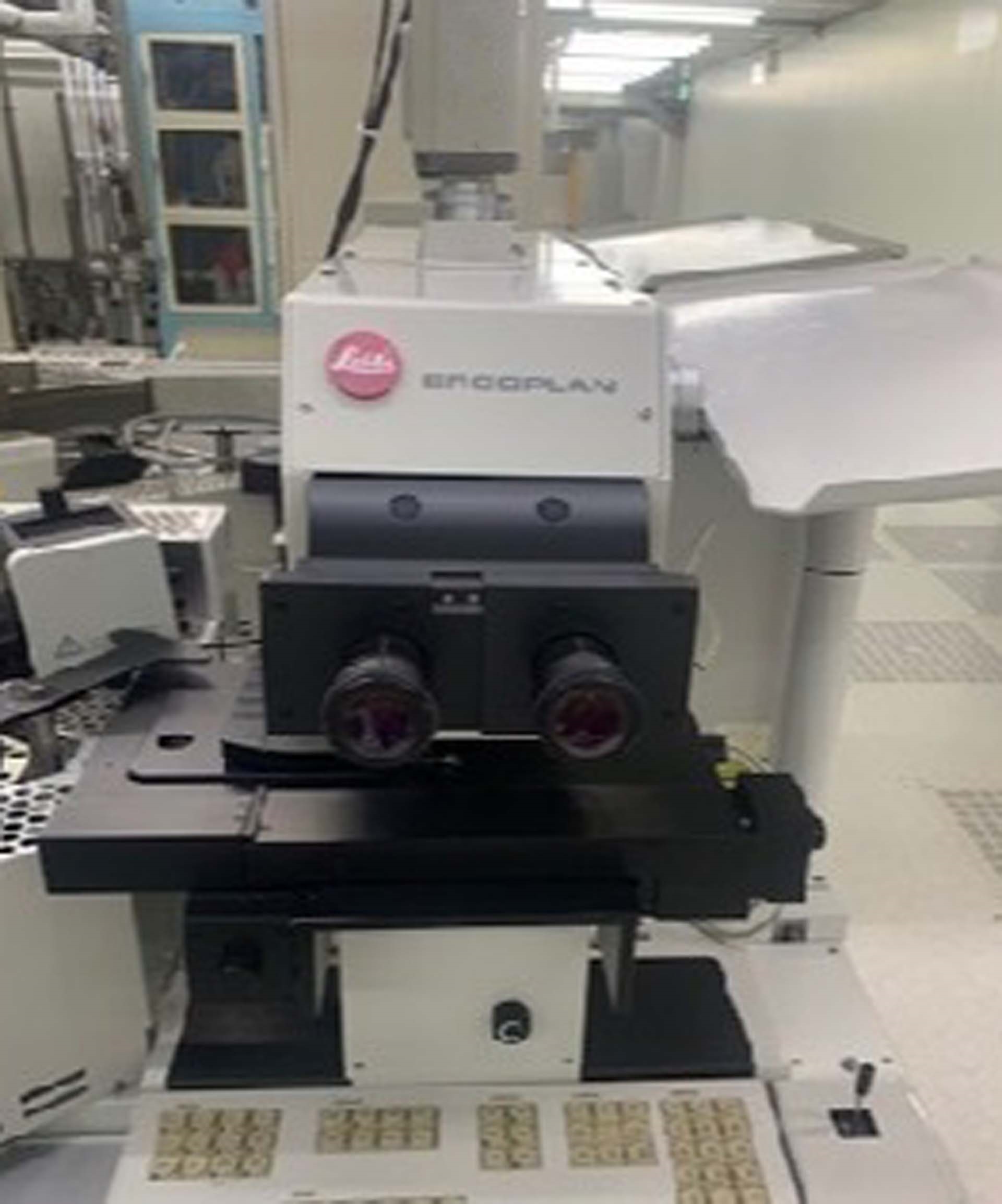

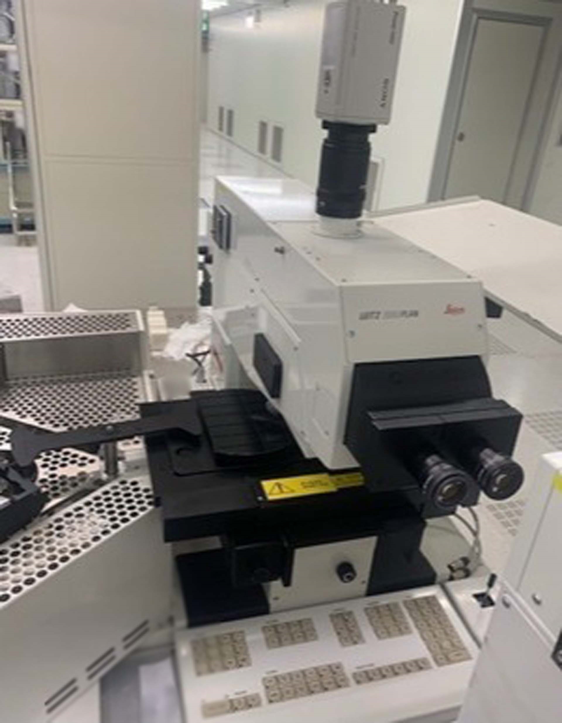

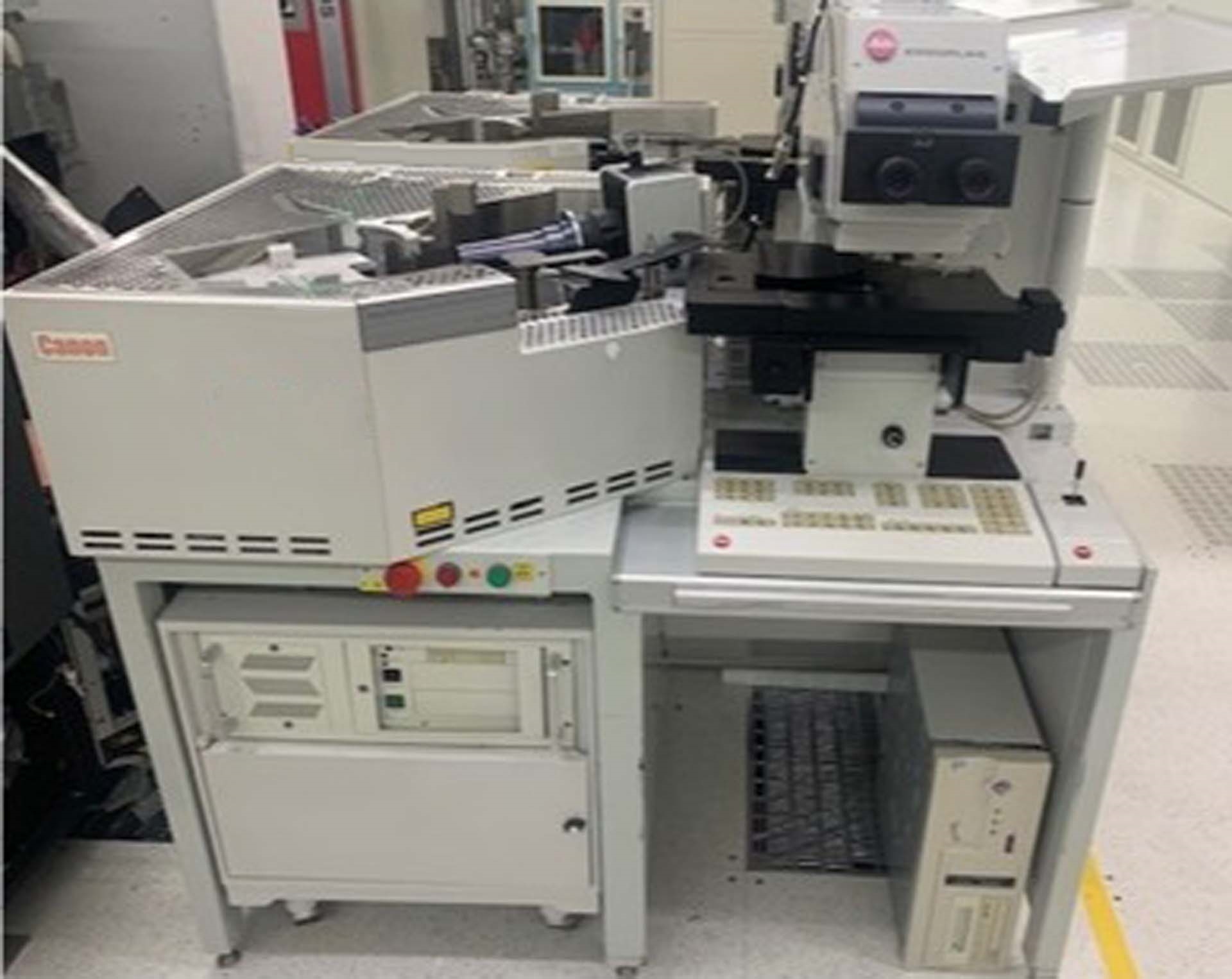

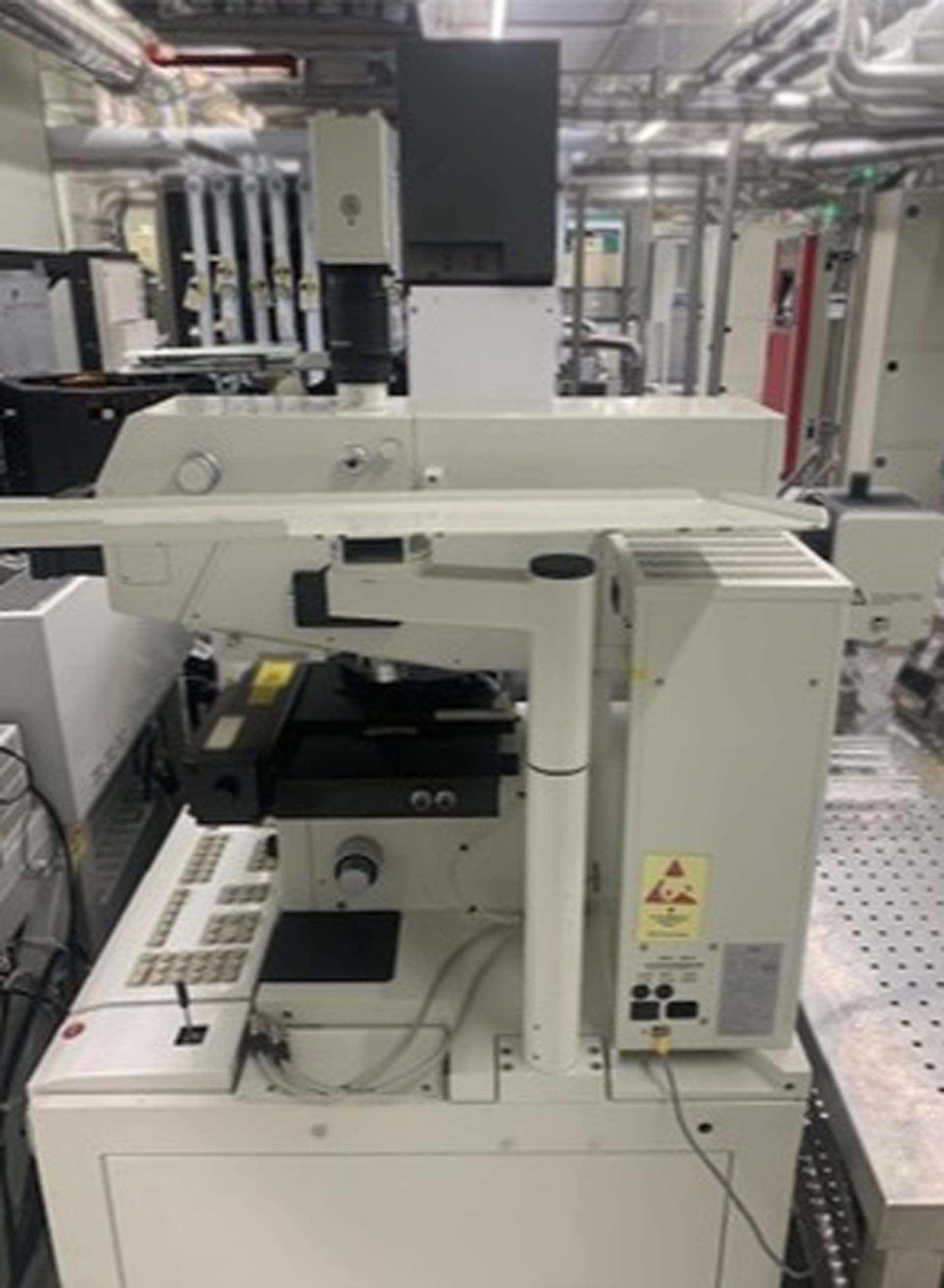

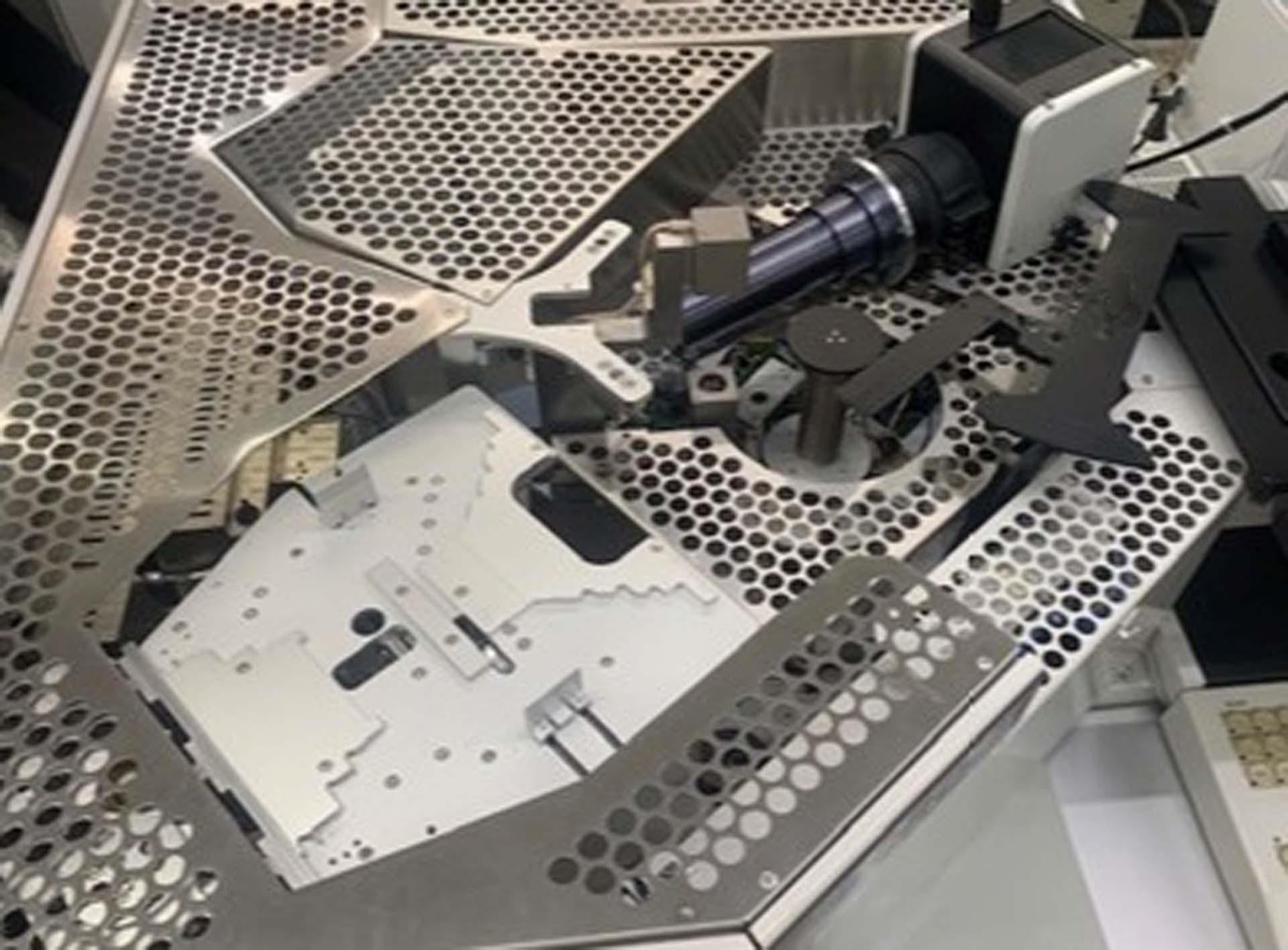

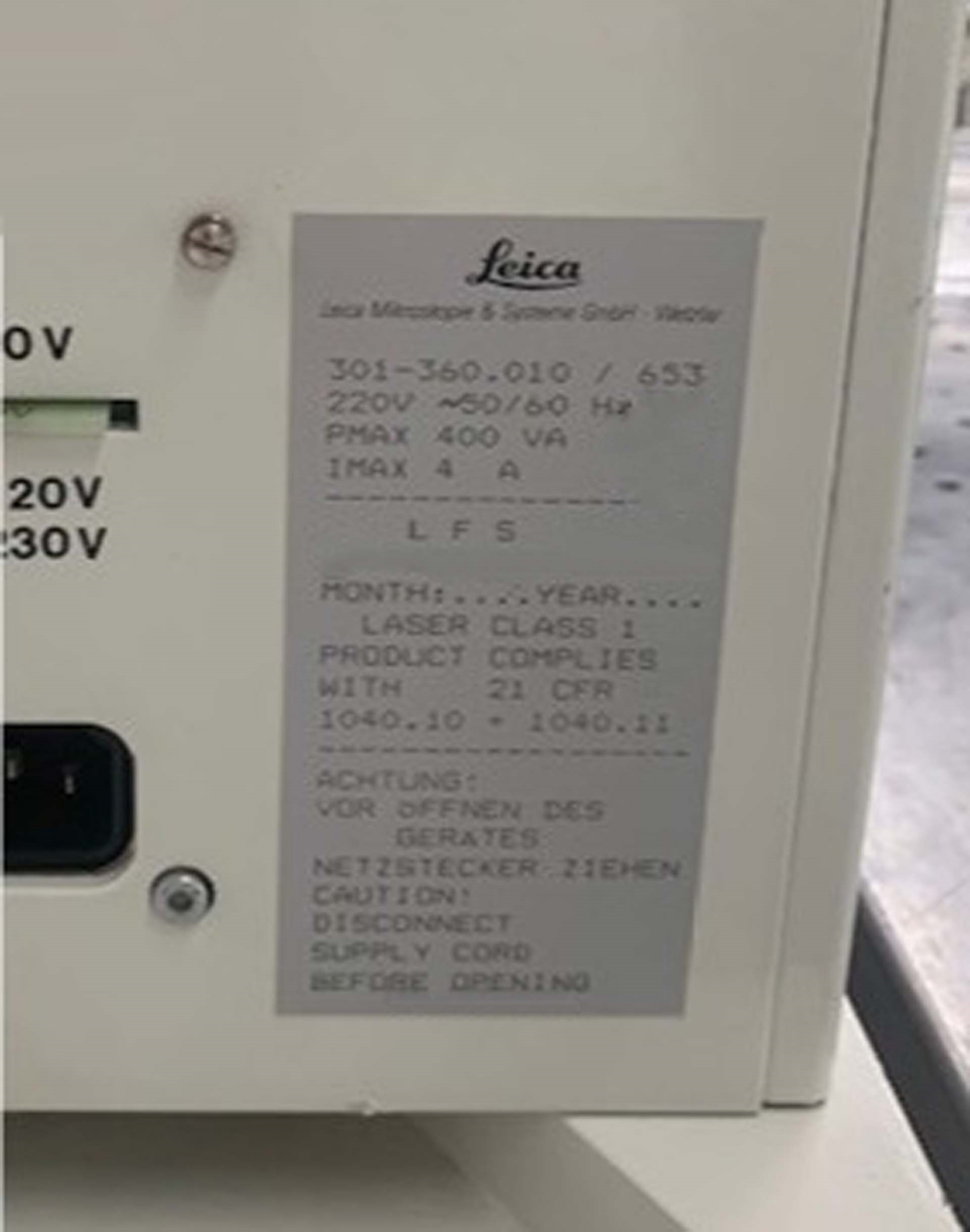

LEICA / VISTEC MIS 200 is a mask and wafer inspection equipment designed for semiconductor production applications. It is a high performance system that allows users to accurately inspect each level of their masks, wafers and other associated materials while minimizing the amount of time and effort required. The unit is composed of a number of components, which work together to ensure efficient and accurate inspections. The key components of LEICA MIS 200 include a high-resolution confocal imaging module, a polarization contrast module, a total reflectance module, multiple visual inspection module, a sample cleanliness inspection module, an alignment station and a software package. The imaging module of the machine is equipped with an advanced high-quality imaging technology to enable accurate inspection of masks and wafers. This module scans images with exceptional clarity and resolves fine details, which enable users to accurately identify and evaluate even the smallest imperfections on the scanned masks and wafers. The polarization contrast module allows the user to examine polarized light on patterns surface without underexposed or overexposed spots. Additionally, this module can detect defects that would usually be missed by standard inspection methods. The total reflectance module is designed for fast, quantitative reflectance mapping on masks and wafers. This module measures reflectance versus film thickness, enabling users to detect small thickness differences between adjacent layers. The multiple visual inspection module is a powerful optical tool that provides users with an enhanced view on defects. This module allows users to identify surface defects of the scanned masks and wafers. Additionally, this module is also capable of identifying damaged electrical connections between the scanned masks and wafers. The sample cleanliness inspection module of the tool enables the user to accurately inspect the cleanliness of their samples prior to inspection. The module detects contaminants, such as dusts and organic debris, enabling the user to remove the contaminants before further inspection. The alignment station of the asset is equipped with laser technologies that ensure precise alignment of the inspected masks and wafers. This reliable alignment will ensure that all scans of the masks and wafers are accurate and consistent. Finally, VISTEC MIS 200 also includes a software package that automates the entire inspection process. The software includes image processing and analysis tools, as well as an intuitive user interface that allows the user to easily monitor and configure their inspection settings. Overall, MIS 200 is a highly advanced mask and wafer inspection model that enables the user to quickly and accurately inspect their masks and wafers for defects. It is an ideal solution for semiconductor production applications.
There are no reviews yet


