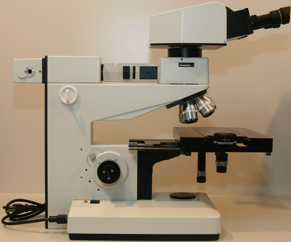
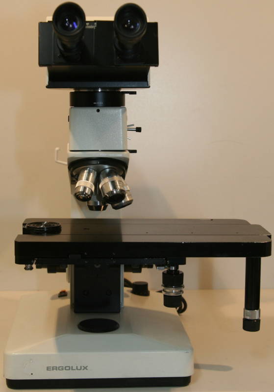
Used LEITZ Ergolux #193173 for sale
URL successfully copied!
Tap to zoom


ID: 193173
Microscope
Includes: 10x, 20x, 50x and 100x and eyepieces
Motorized Turret.
LEITZ Ergolux mask & wafer inspection equipment for semiconductor imaging is a unique system that provides industry leading accuracy and efficiency for the inspection of silicon wafers and masks. This unit utilizes a unique robotic imaging platform with integrated advanced vision and metrology capabilities. Ergolux machine has been designed to provide an effective, non-destructive imaging environment that reduces both the likelihood of wafer and mask damage as well as the amount of time and resources spent with traditional inspection methods. LEITZ Ergolux is designed to be operator friendly and includes intuitive user interfaces for quickly setting parameters and configurations. The Automated Tool Control (ASC) software provides programming tools for easily stetting up automated measurement cycles, with user-friendly graphical programming elements. With the integrated Vision and Metrology systems, operators can quickly define and adjust measurement patterns and when combined with the extensive measurements result extraction capability, comprehensive non-destructive failure analyses of wafers and masks can be conducted with confidence. Ergolux includes advanced stereo vision capabilities, such as multi-axis scan, zoom, pan, tilt, scan deck rotation, scan area projection and image alignment correction. The multi-axis image scan eliminates motion artifacts commonly observed in traditional manual or scanner inspections and allows for tighter, accurate measurements to be conducted over different wafer and mask geometries. The zoom and pan functions allow for larger images to be captured and inspected, which provide greater detail in defect analysis. The optical microscope on LEITZ Ergolux platform provides an in-depth analysis for any potential defects or anomalies that have been identified in an image. The microscope also has replaceable objective lenses to further assist the operator in identifying complex defects such as resist image distortion, wire breakages or short circuits in large scale integrated circuits. Additionally, the microscope can be used to examine both the front and back sides of a wafer or mask for further failure analysis. Furthermore, Ergolux includes an automated Non-Destructive Wafer Stress Analyzer which is designed to measure the strain levels of any wafers or masks during the inspection process. The NDSSA is a non-contact asset that uses HPS™ high-precision sensors to map the stress of the surface of a wafer or mask. This stress analysis measurement can be used to detect small changes in a wafer or mask and provides a comprehensive overview of a wafer or mask to ensure defect-free manufacturing. LEITZ Ergolux is an innovative imaging model that is ideal for semiconductor imaging applications. The advanced imaging capabilities, automated wafer stress analysis and intuitive user interfaces provide efficient, accurate inspection results that meet the most demanding process requirements. Ergolux equipment is designed for demanding production environments and will provide robust results for the semiconductor inspection process.
There are no reviews yet

