Used METRICON 2010/M #293767526 for sale
URL successfully copied!





Tap to zoom


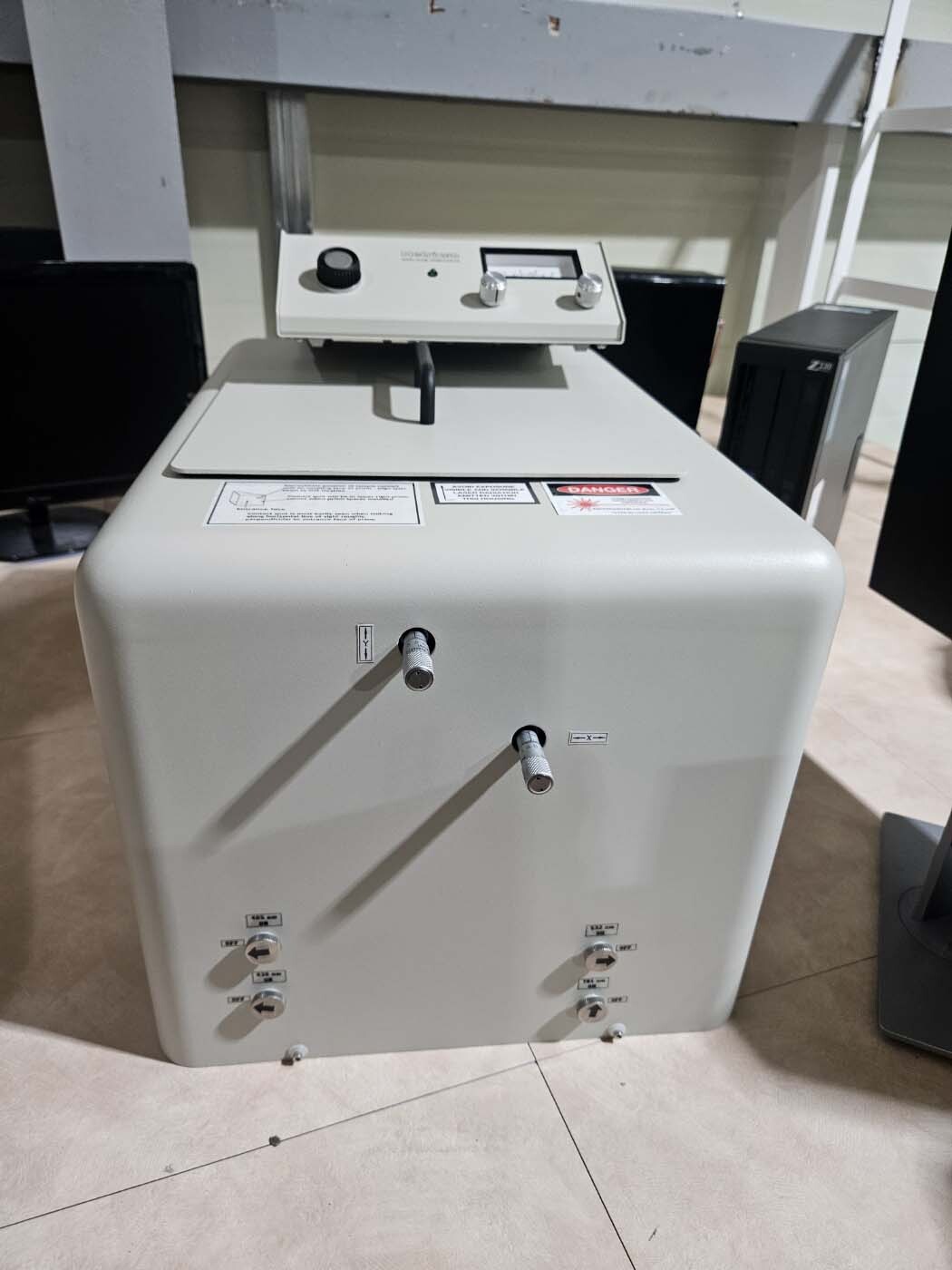


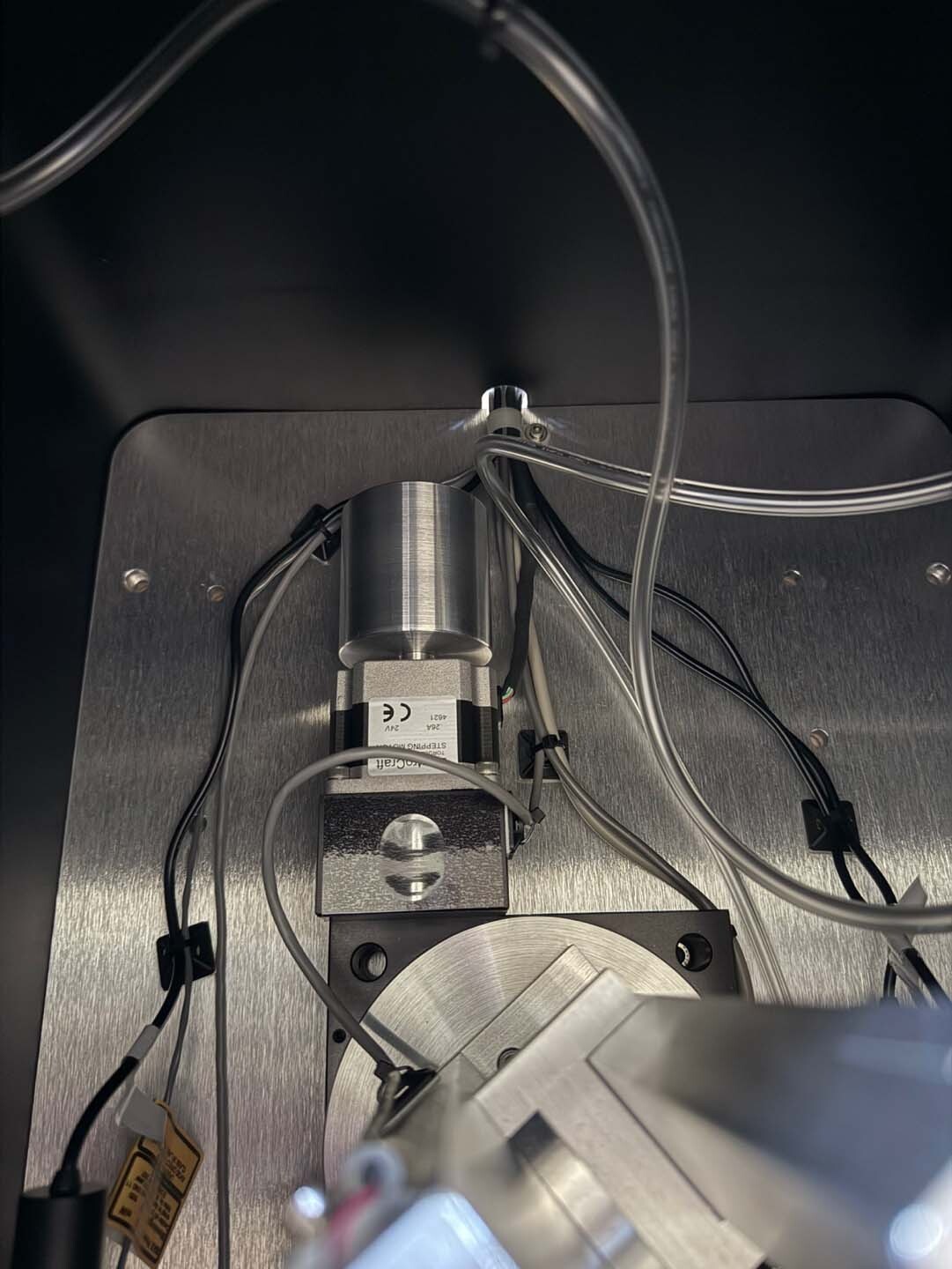

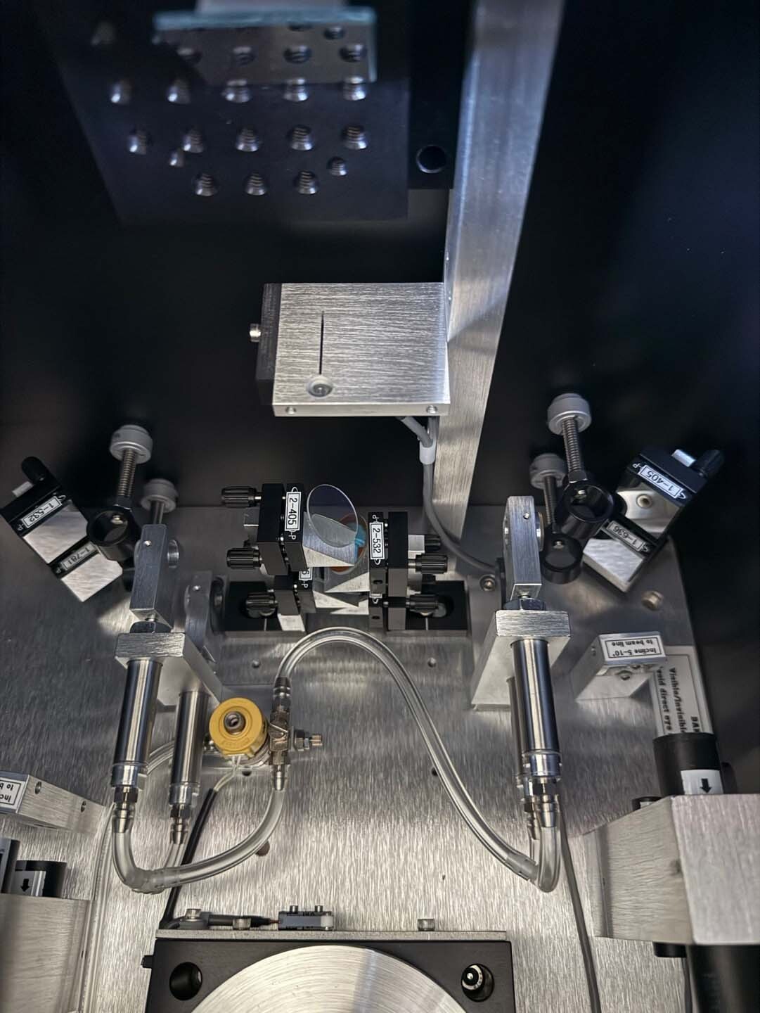

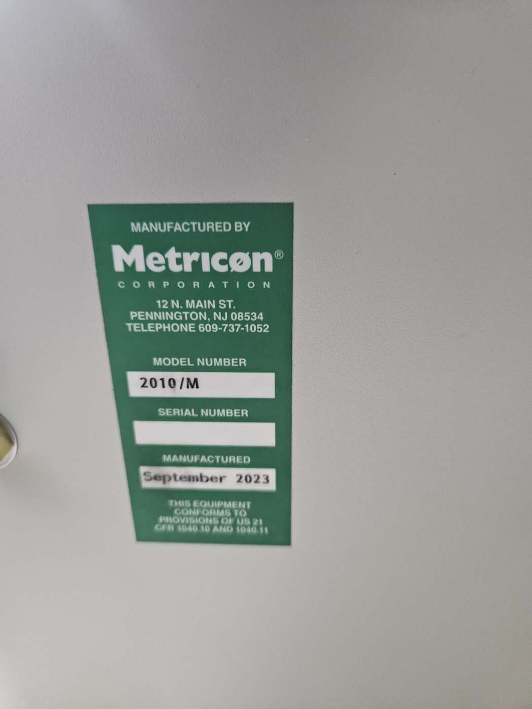
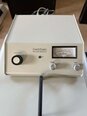
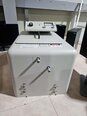
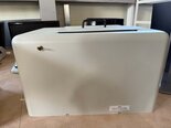
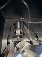
METRICON 2010/M is a powerful wafer and mask inspection equipment designed to provide high throughput and high resolution capabilities for demanding wafer and mask requirements. The system utilizes advanced image processing and imaging technologies to inspect wafer and mask patterns and defects at subpixel levels. It features a large and resolution-rich imaging unit with a two-dimensional image sensor for high throughput and accuracy at all purposes. It is equipped with optics and a dual-beam pattern comparator for comparing multiple patterns for consistency and defects. As well as this, its proprietary imaging software optimizes the speed and accuracy of image processing and feature extraction, allowing customized inspection methods to be created for specific wafers or masks. The machine also offers flexibility with its modular design, allowing the configuration to be adjusted to suit the process requirements. Its software architecture is modularized and highly parallelized, allowing for efficient control of inspection order or flow for improved throughput. Plus, it supports a range of devices including non-patterned wafers, masks with complex geometries, and grating structures. In addition, METRICON 2010/M includes integrated operations and test controls for improved accuracy and tracking of results. This ensures that all process and inspection parameters such as fan-out and layer time are recorded and monitored for reliability and improved process control. The tool also includes graphical user interface controls for easy operation and can link to the image inspection environment. METRICON 2010/M is an excellent tool for Inspection and Test of highly complex wafer and mask patterns. It provides users with superior image resolution compared to other systems, excellent flexibility and control both in the configuration and in the integrated operations and test controls. These capabilities allow for improved process control, improved detection of defects, and improved yield gains. As a result, it is ideal for the automated and precise inspection of wafer and mask structures.
There are no reviews yet