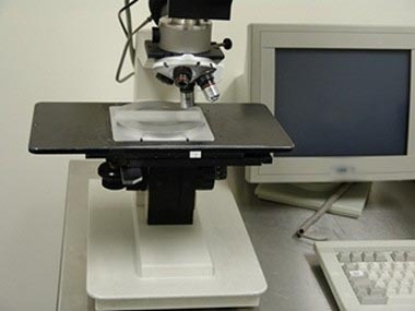
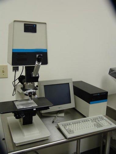
Used NANOMETRICS 210 #9123978 for sale
URL successfully copied!
Tap to zoom


ID: 9123978
Wafer Size: 1-6"
Thin film thickness measurement systems, 3"-6"
Includes:
Photoresists
Polyimides
Polysilicon
Oxides
Nitrides
Ranges: 100A to 500kA
Measurement time: 2.5 seconds.
NANOMETRICS 210 is a mask and wafer inspection equipment ideal for use in semiconductor manufacturing and inspection. This system uses a state-of-the-art spectral imaging scanning algorithm to deliver fast and accurate inspection results. The unit provides two independent inspection modes, a high resolution mode and a high dynamic range mode, allowing users to inspect a wide range of substrates with detail and clarity. 210 machine includes an advanced optical tool composed of advanced optical components, such as objective lenses, light-shields and illumination sources. This optical asset has an excellent resolution of 0.5µm, ensuring accurate and reliable results. Moreover, the model's optical equipment utilises slit-scanning and field-scanning for high-speed, in-depth data collection. In addition, NANOMETRICS 210 system integrates an innovative monochrome bimolar chain imaging algorithm. This algorithm enables the unit to detect defects in patterns and dimensions of a wide range of substrates, including transparent, metallic and grey scale. The combination of the optical machine and imaging algorithm ensures accurate and fast image processing. This combination enables the tool to generate high-resolution images with a range of over 10µm and excellent dynamic range. Furthermore, the asset is equipped with a modular software suite, capable of analysis and defect inspection. Its software includes tools for mask inspections and defect classification, defect level measurement and review, and the ability to select, localize and measure defects while maintaining low false-alarm rates. 210 has been designed to meet the requirements of the semiconductor production. The model offers fast throughput, high resolution, accuracy, low false-alarm rates, and a variety of analytical techniques implemented within its software. These components, together with a wide range of substrates and defect types it can inspect, allows for fast and accurate, high-yield semiconductor production.
There are no reviews yet

