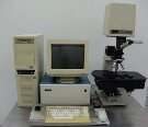
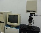
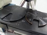
Used NANOMETRICS 4150 #9124007 for sale
URL successfully copied!
Tap to zoom
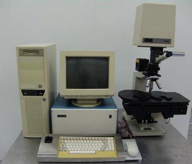

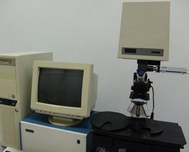

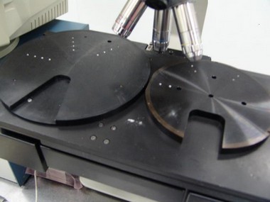

ID: 9124007
Wafer Size: 6"-8"
Vintage: 1994
Reflectivity & mapping system, 6"-8"
Film thickness
Single and multiple layer measurement programs
Ability to select film constants
Scan ranges and substrate types
High speed auto-focus torret style objectives head
MSPlan 5
MSPlan 10
MSPlan 50
Reflecting objective x15
Programmable mapping stage: Accuracy +/- 2 mm data analysis
Motorized stage
Stage accuracy: 2mm High resolution contour
3D Mapping
Pulnix TMC-7 camera rapid measurement program development extensive data management SPC capabilities
Mapping: Contour 2D & 3D
115VAC, 5A,50/60Hz
1994 vintage.
NANOMETRICS 4150 is a mask & wafer inspection equipment that is widely used in the semiconductor industry. It helps to ensure that masks and wafers meet critical tolerances and are free of defects. The system offers two inspection capabilities: static imaging and dynamic imaging. The static imaging is used to identify gross defects such as built-in charges, voids, delamination, and a variety of contaminants. It does this by detecting light reflected off the surface of the mask or wafer. Dynamic imaging is used to identify fine defects which may not be visible to static imaging, such as particles or foreign material in the film or substrate. The unit is equipped with a series of advanced features to ensure the accuracy of inspection. For example, it uses a high-speed X-Y stage with servodrives to move the sample across the camera, providing a fast and precise positioning. The Sub Micron Step Profile Measurement option is designed to detect curvatures in the surface of the sample within a range of 0.1-100 μm. Additionally, the Nanometric Pattern Match Tool is used to measure nanoscale differences between two masks or between two different layers of a wafer. The optics used in the machine are highly sensitive and highly precise, capable of detecting features between 0.5-2 μm. The backside imaging option further allows for the inspection of external layer structures while a special detector setup helps to optimize signal-to-noise ratio. The tool's user interface is designed to provide a simple and intuitive operation for quick inspection. Its real-time multi-window and split-window technology allows inspect multiple samples simultaneously, while its three-dimensional user interface allows for better visuals to classify defects. Overall, 4150 asset offers advanced features for accurate and efficient defect inspection in masks and wafers. This helps users to ensure product integrity and reduce waste, ultimately resulting in cost savings.
There are no reviews yet
