Used NANOMETRICS 7000-033895 #9242378 for sale
URL successfully copied!
Tap to zoom



















ID: 9242378
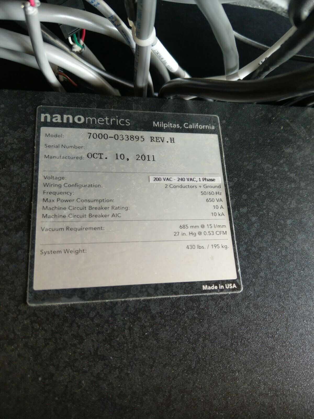
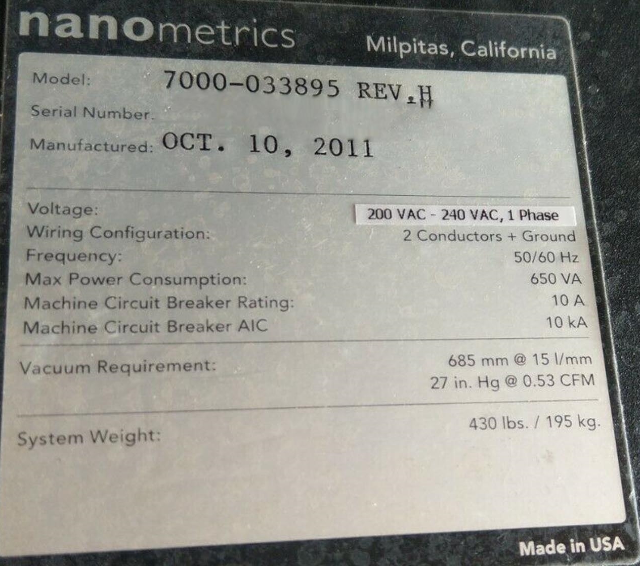
Vintage: 2011
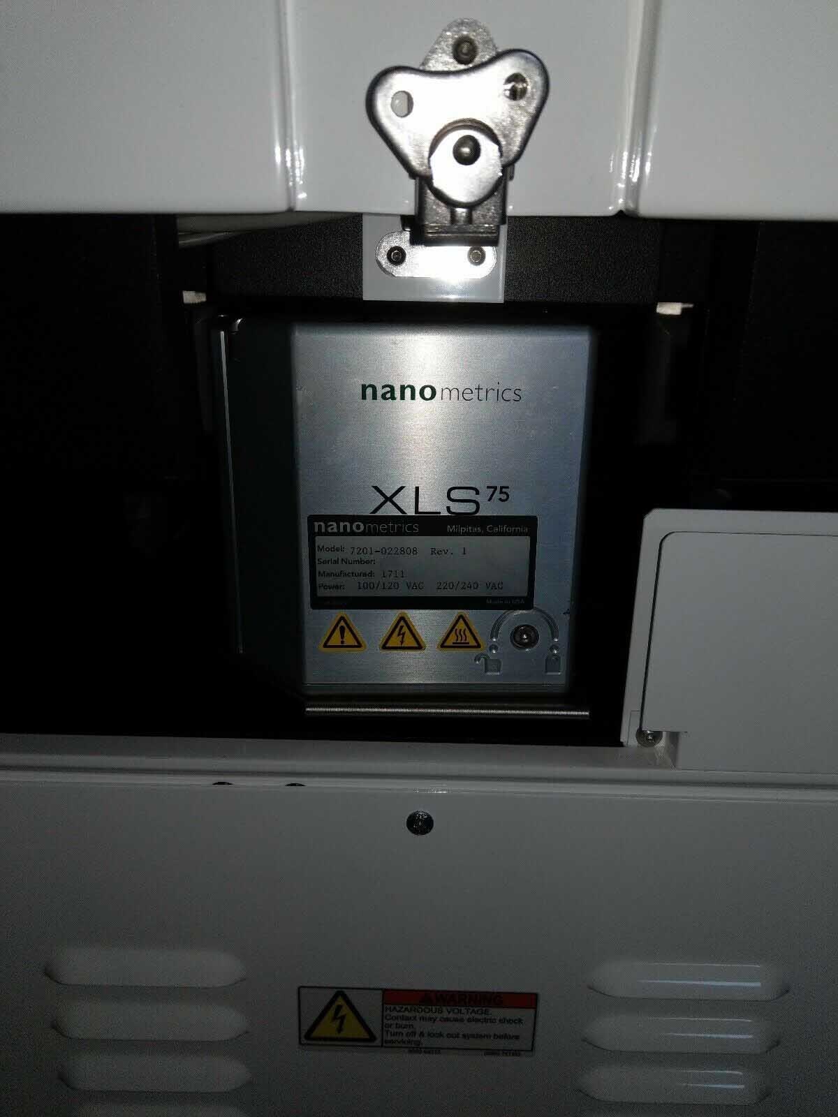
Integrated metrology OCD / Film analysis system
2011 vintage.
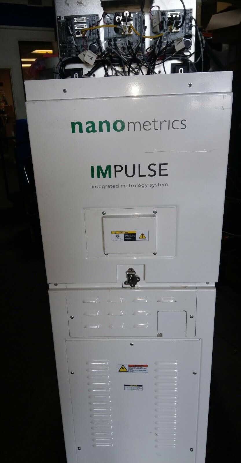
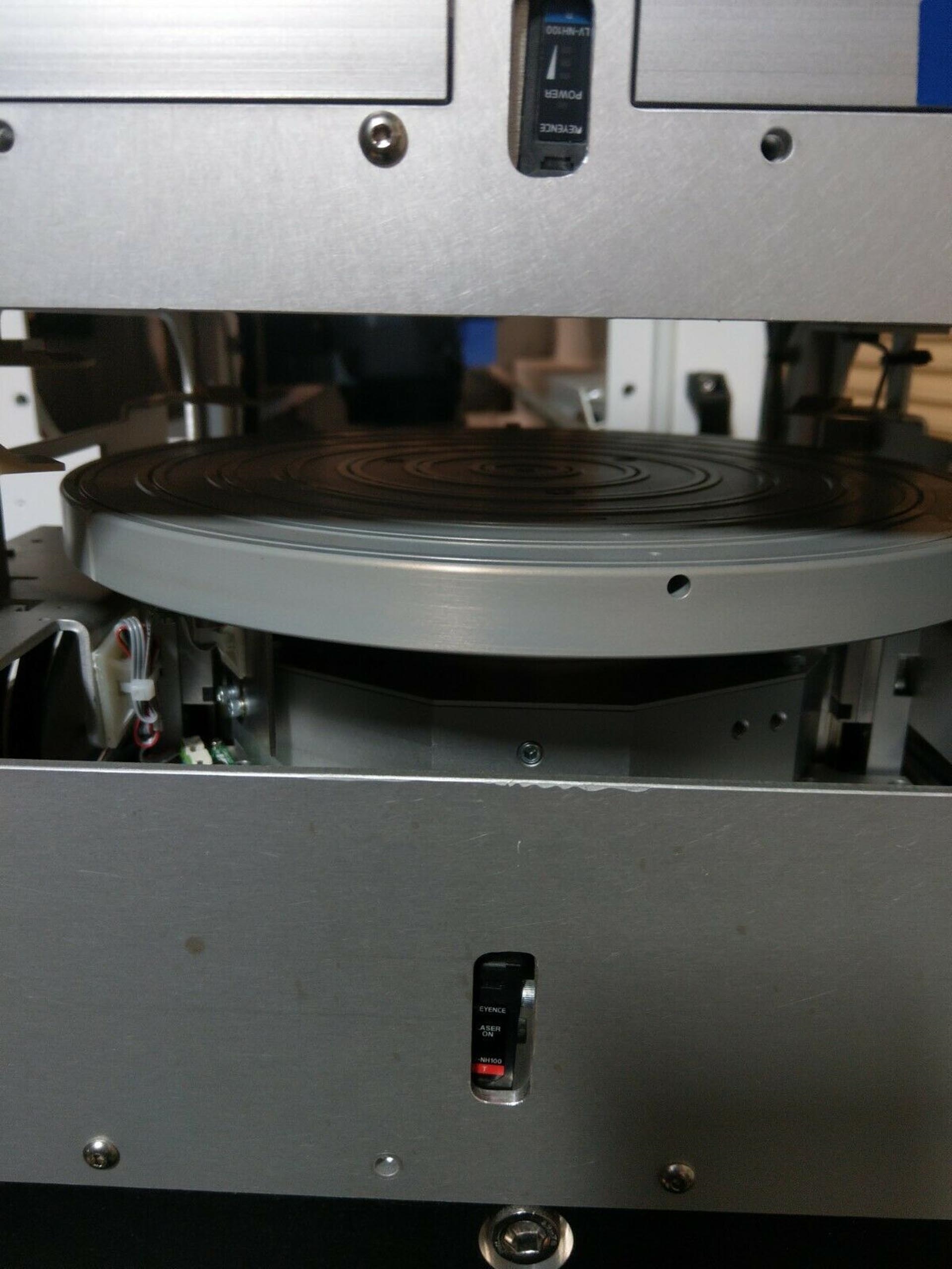
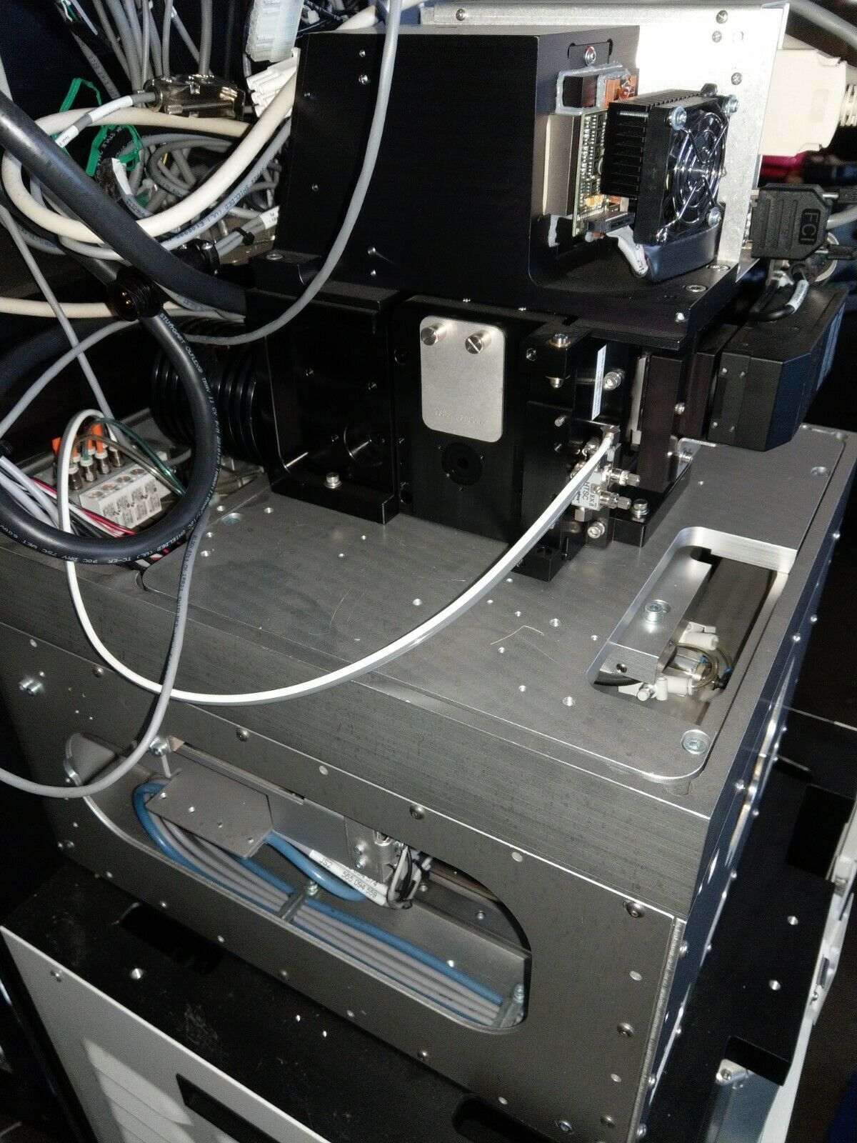
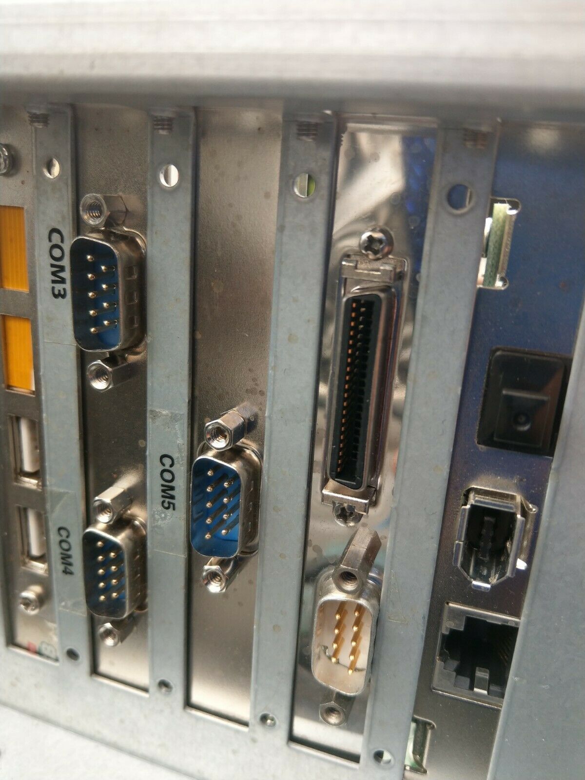
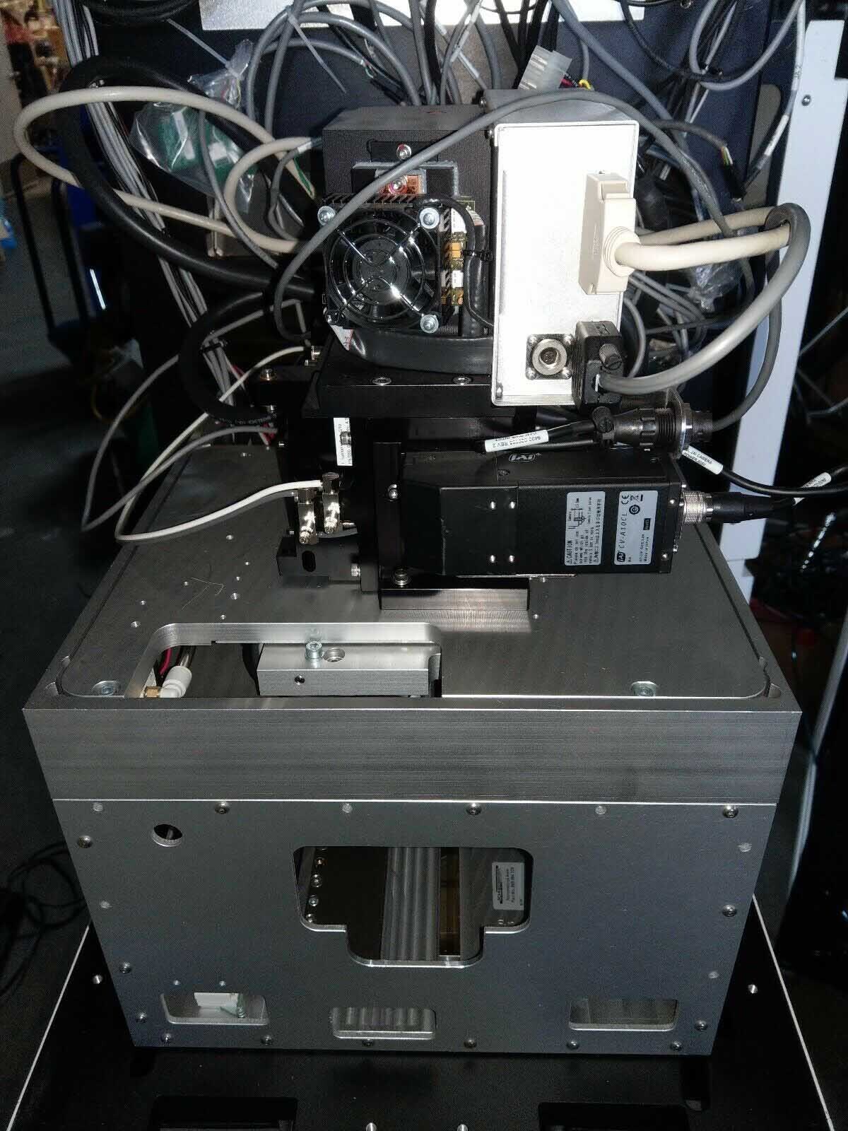
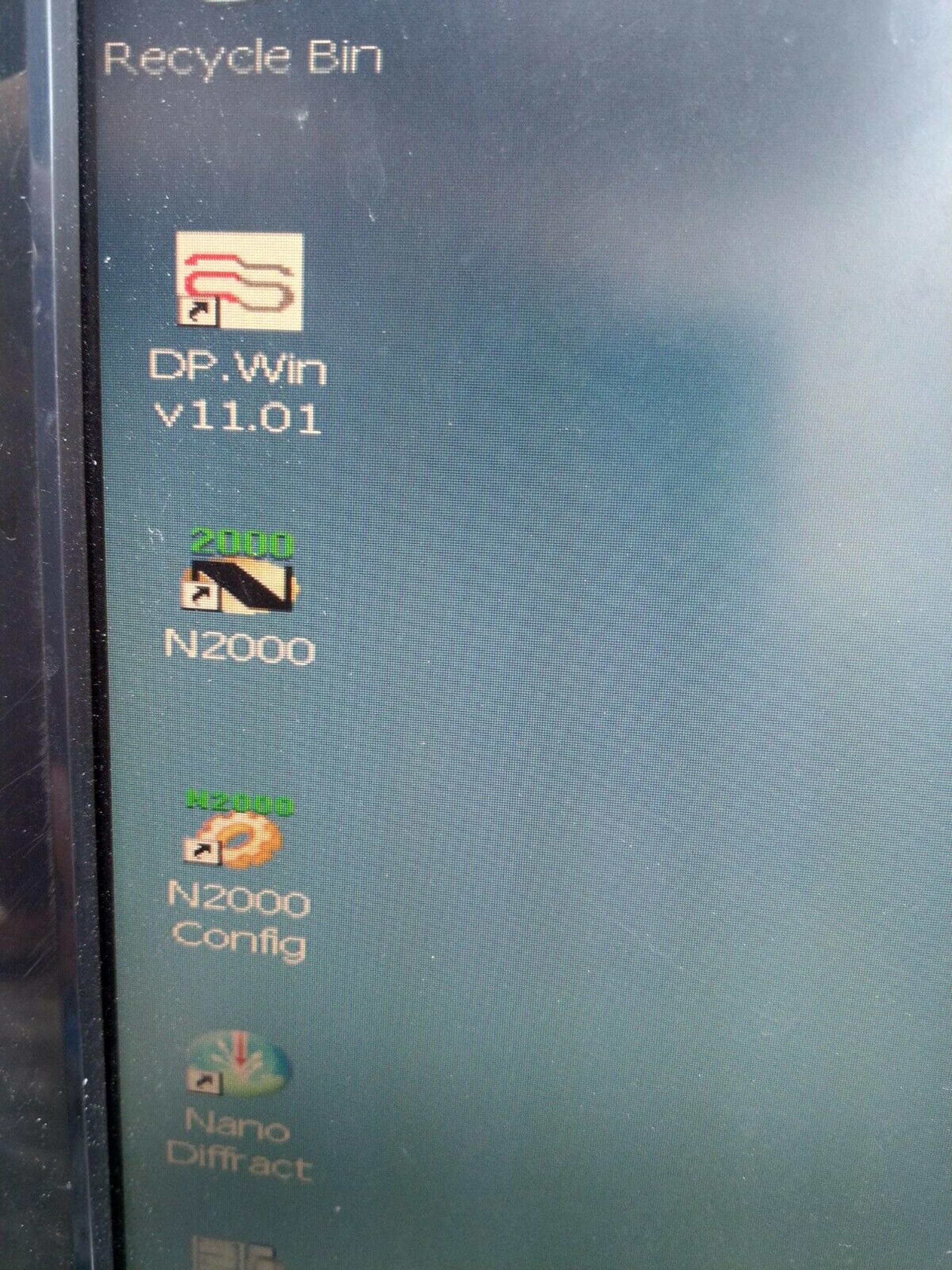
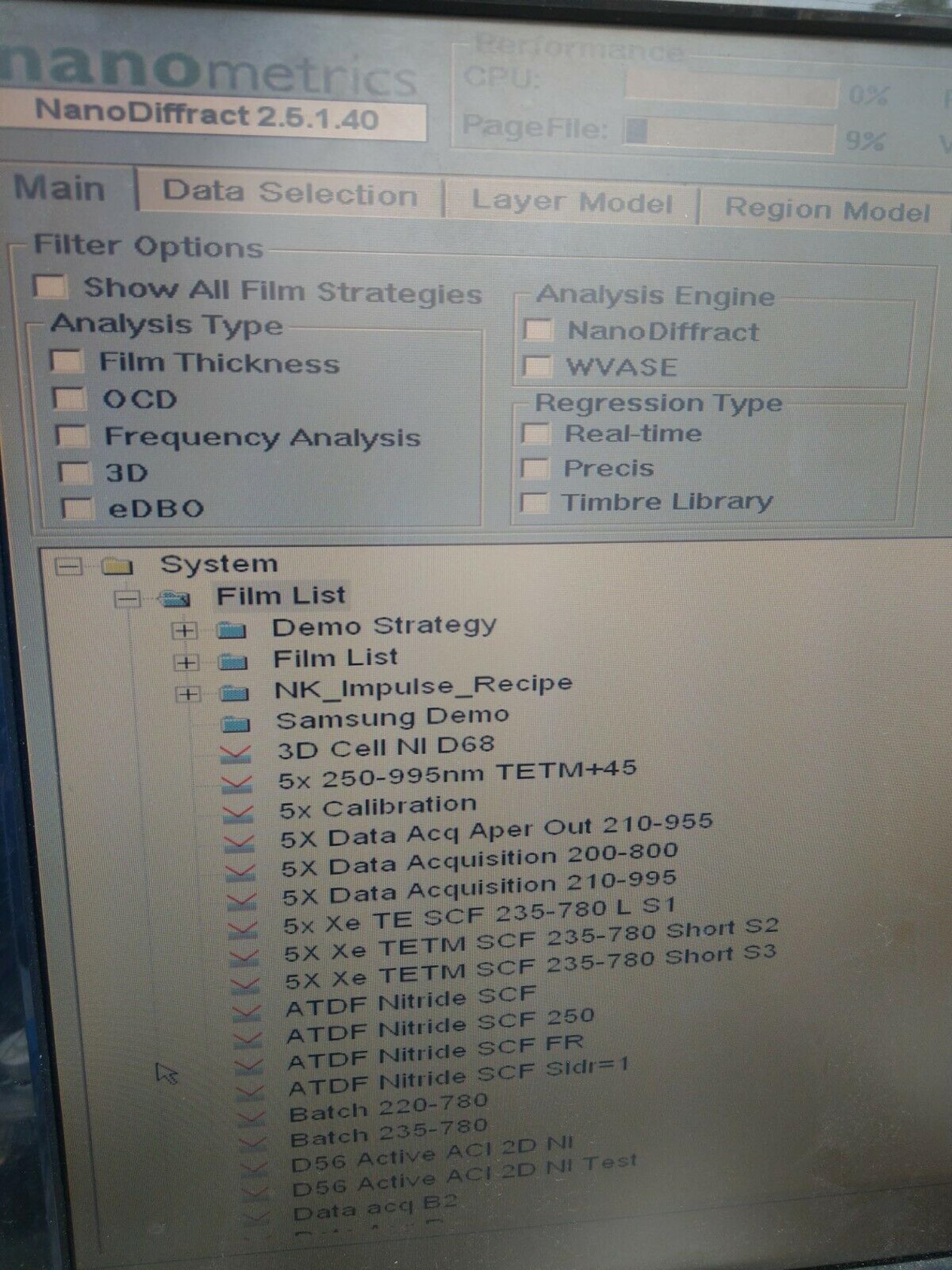
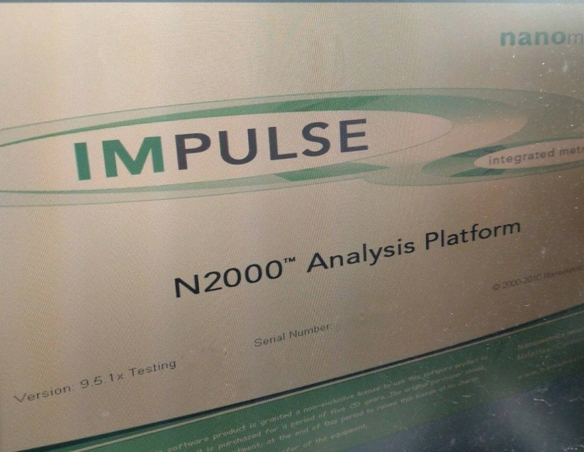
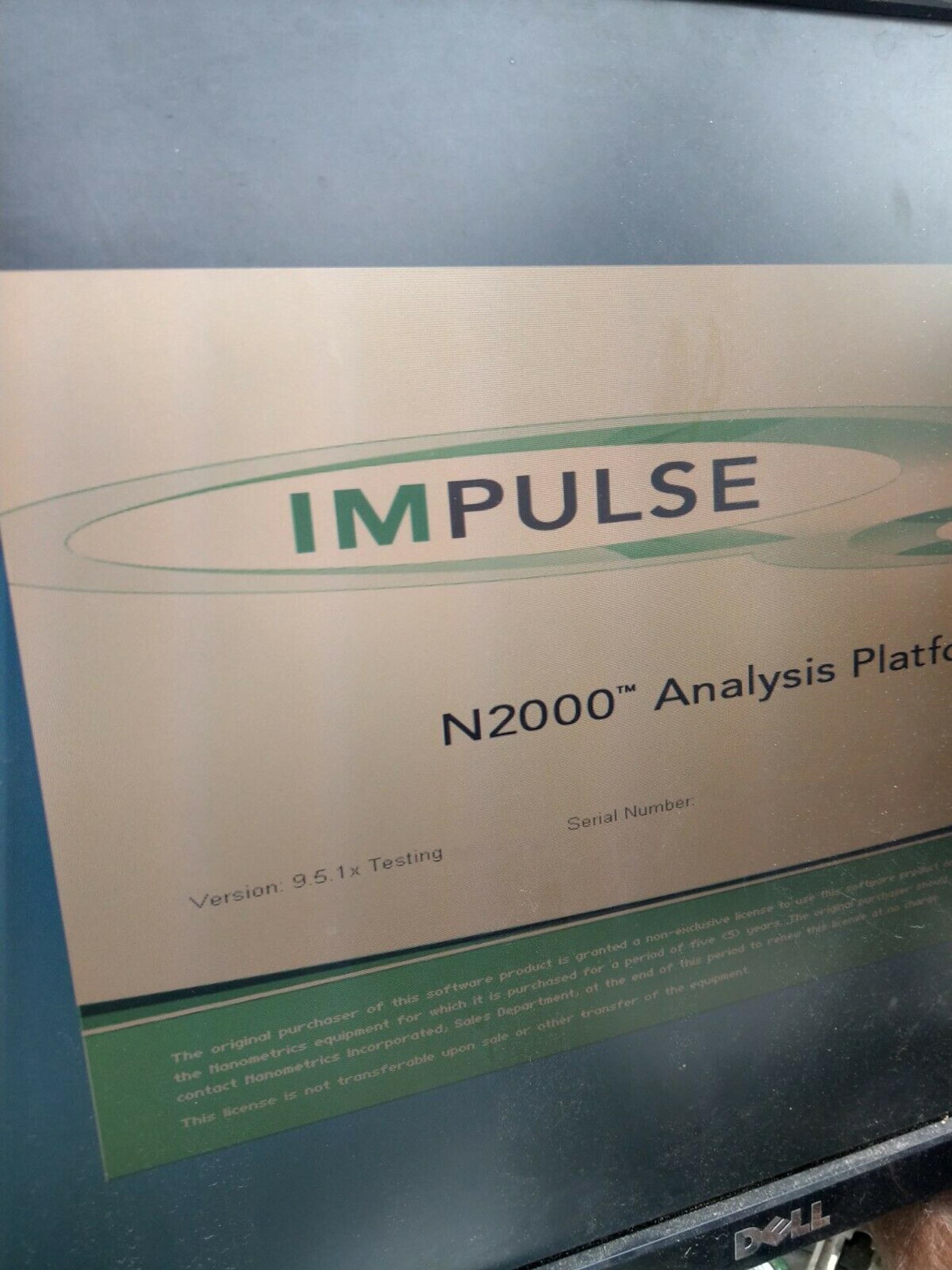
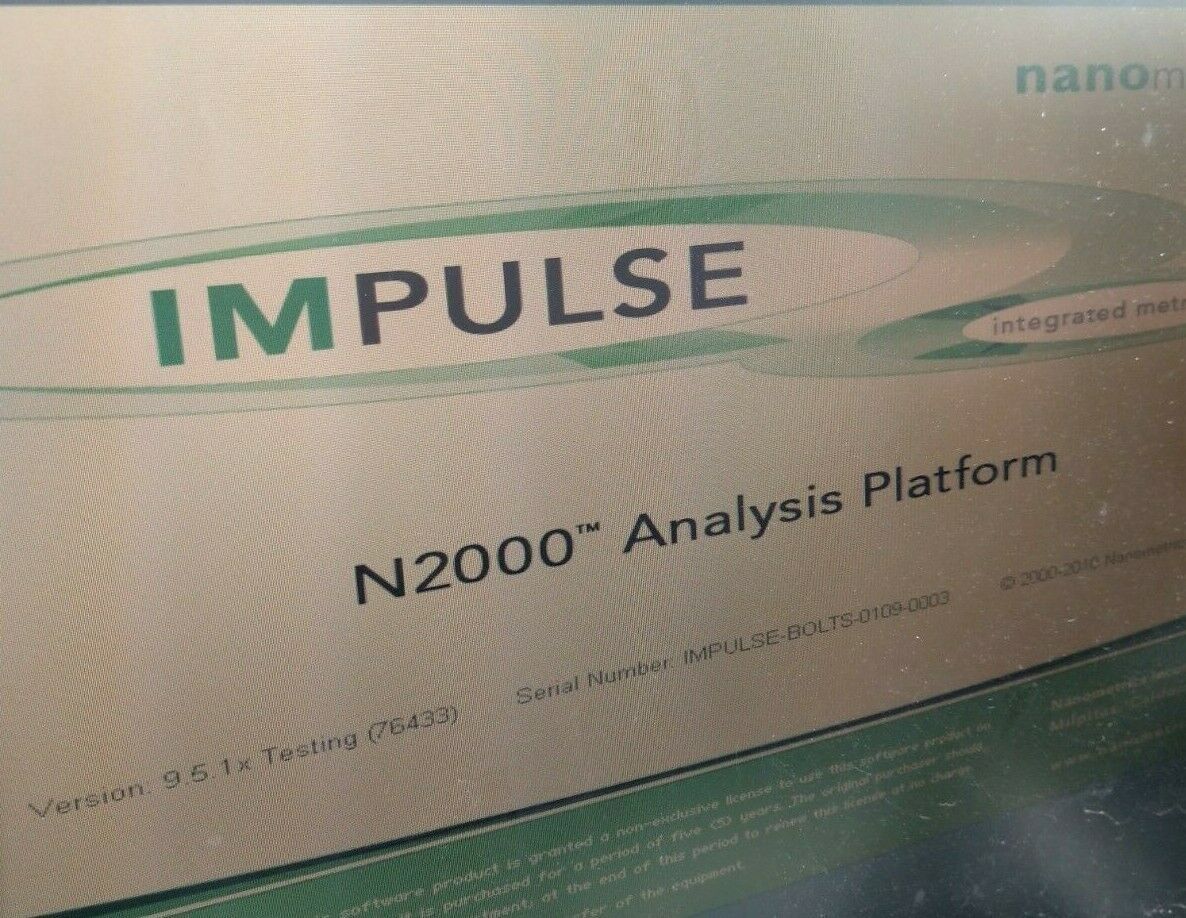
NANOMETRICS 7000-033895 'Mask & Wafer Inspection' equipment is a high-performance optical inspection tool used in the production of integrated circuits. It is designed to provide fast and accurate image-based analysis of contact layer features for both reticles, or masks, and wafers. The system comprises the mainframe, stage, and optics unit. The mainframe is a multi-functional, workhorse platform that houses the stage, opto-electronics, precision motion control systems, and user interface. The mainframe is designed to provide reliable, efficient use with a wide range of image capture and analyses features. The stage is a precision air-bearing platform, able to locate precisely and smoothly on the x and y axes using a combination of encoder technology and linear optical encoders. It is also built with a precision-motor-driven machine, allowing for precise positioning of the Mask & Wafer substrate. The optics tool is designed to provide high-resolution imaging (up to 22 million pixels) of contacts layers on substrates. The entire asset is housed in a non-reflective black environment, allowing for greater precision with minimal optical reflections. The optics also contains several high-power lasers and super lenses for the illumination of the masks and wafers. The precise positioning of these components greatly improves the performance of the model. The onboard software allows for the automatic detection of contact layer features with a high degree of accuracy. Additionally, the software supports object-oriented measurements and computer-aided design software (CAD) which enables the user to both analyze and place a great number of contact features on a single substrate with a single image. With this level of accuracy computations, design simulations, and evaluations might be achieved. Finally, the equipment is compliant with most industry standards and is capable of verifying contact features to 20nm, which is smaller than a wavelength of visible light. This is incredibly advantageous for the production of advanced integrated circuits. This system uses the best available components and software functions to deliver robust and consistent results with high accuracy, making it the ideal tool for any contact layer inspection job.
There are no reviews yet


