Used NANOMETRICS NanoSpec 3000 #293772245 for sale
URL successfully copied!
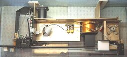
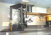
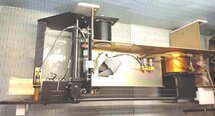
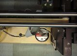
Tap to zoom
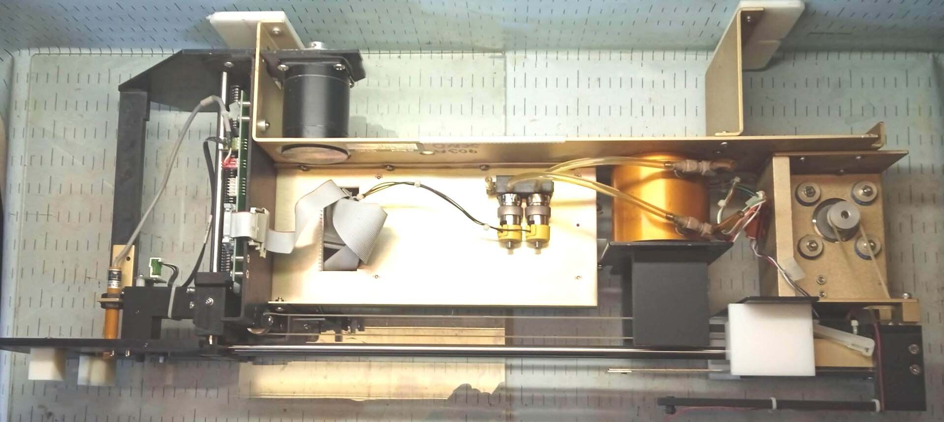

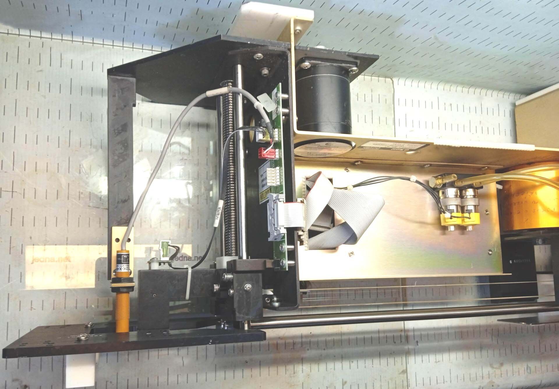
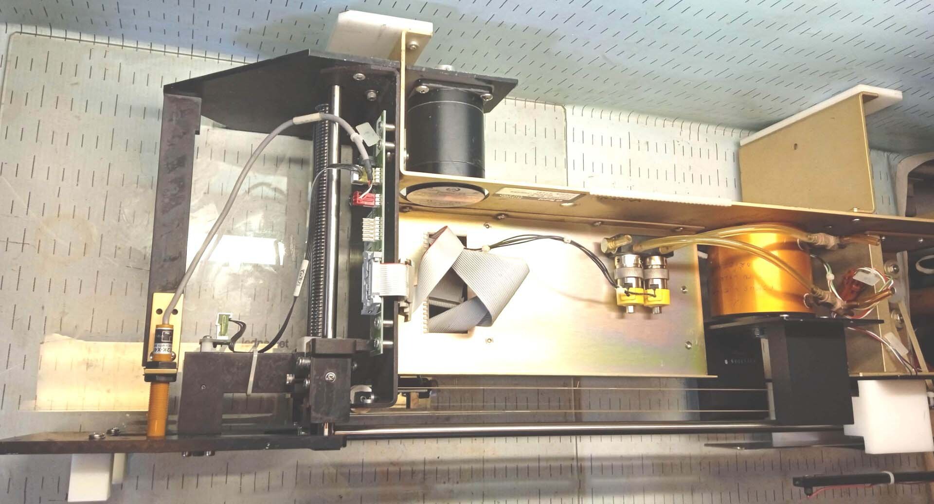
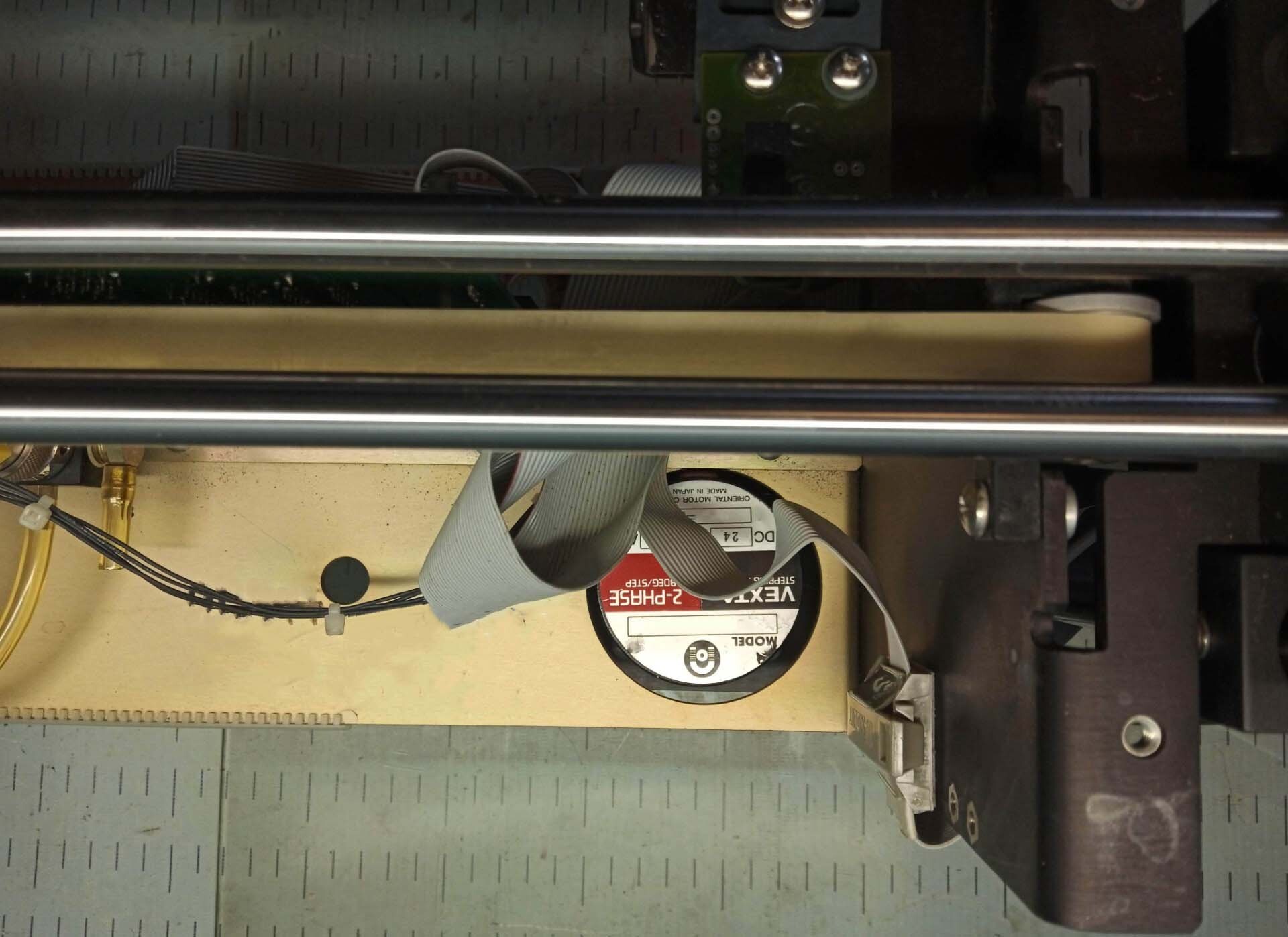
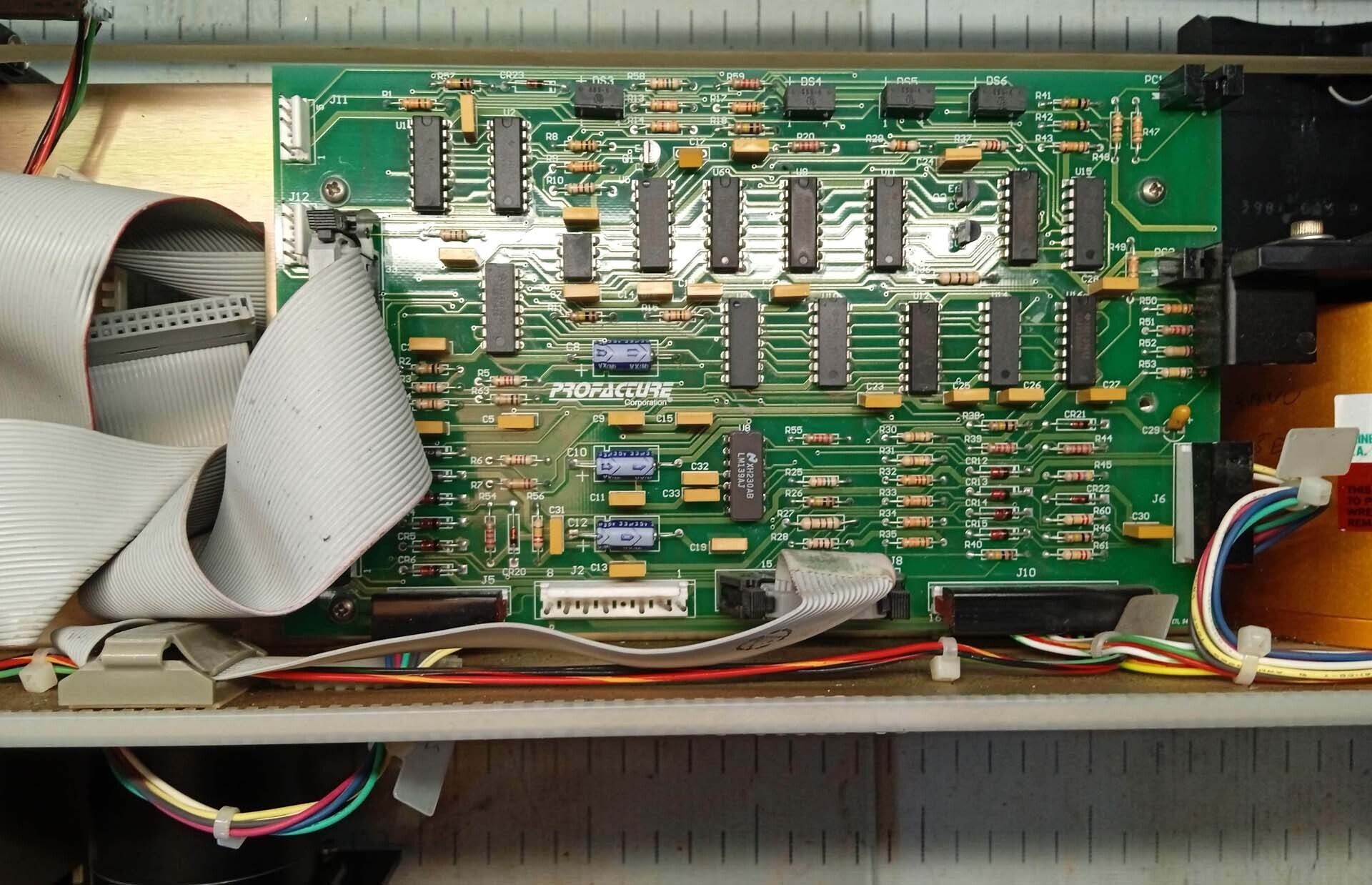
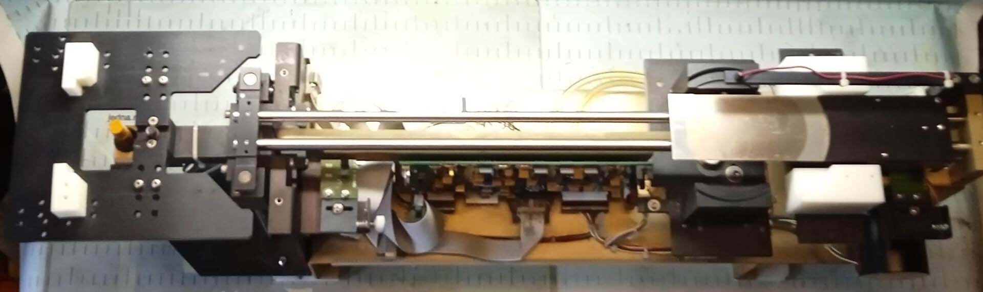
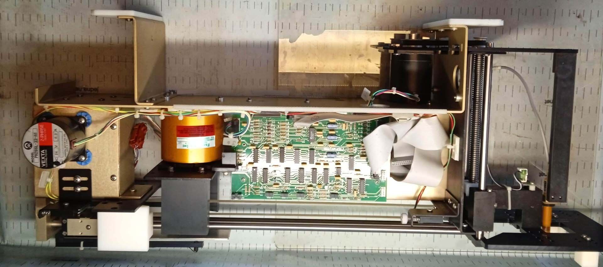
NANOMETRICS NanoSpec 3000 is an advanced mask and wafer inspection equipment that sets the industry standard for high-performance semiconductor inspection and metrology. NanoSpec 3000 is designed to provide accurate and reliable measurements for critical process control in semiconductor manufacturing, enabling manufacturers to achieve consistent yields and ensure the quality of their products. This innovative system integrates state-of-the-art technology with advanced algorithms to deliver unmatched precision and efficiency in semiconductor inspection. At the heart of NANOMETRICS NanoSpec 3000 is its cutting-edge optical inspection technology, which combines bright-field, dark-field, and differential interference contrast (DIC) imaging techniques to deliver superior image quality and resolution. These imaging techniques enable the unit to capture detailed images of semiconductor features with sub-nanometer precision, allowing for precise detection of defects and anomalies on masks and wafers. The machine is equipped with high-resolution cameras and advanced image processing capabilities that enhance image clarity and contrast, enabling accurate defect detection and classification with exceptional sensitivity. One of the key features of NanoSpec 3000 is its advanced defect detection algorithms, which are designed to identify and classify defects on masks and wafers with unmatched accuracy and reliability. The tool is capable of detecting a wide range of defects, including particles, scratches, patterning errors, and contamination, enabling manufacturers to quickly identify and rectify process issues that could affect yield and product quality. The asset's automated defect classification capabilities streamlines the inspection process, reducing the time and resources required for defect analysis and resolution. In addition to defect detection, NANOMETRICS NanoSpec 3000 offers comprehensive metrology capabilities for critical dimension measurements on masks and wafers. The model utilizes advanced imaging and measurement algorithms to accurately measure feature dimensions, overlay alignment, and other critical parameters with sub-nanometer resolution. These metrology capabilities enable manufacturers to monitor critical process parameters and ensure the dimensional accuracy of semiconductor features, contributing to improved yield and device performance. NanoSpec 3000 is designed for high-throughput semiconductor manufacturing environments, with fast scan speeds and high inspection efficiency to meet the demanding requirements of modern semiconductor fabrication facilities. The equipment features a user-friendly interface that provides intuitive operation and flexible inspection workflows, allowing operators to easily configure and customize inspections for different mask and wafer types. The system's advanced automation capabilities further enhance productivity by minimizing operator intervention and downtime, enabling continuous inspection and monitoring of semiconductor processes. Overall, NANOMETRICS NanoSpec 3000 is a state-of-the-art mask and wafer inspection unit that offers unparalleled performance, accuracy, and efficiency for semiconductor manufacturing. With its advanced optical inspection technology, defect detection algorithms, and metrology capabilities, NanoSpec 3000 provides manufacturers with the tools they need to ensure the quality and reliability of their semiconductor products while optimizing production processes for maximum yield and efficiency.
There are no reviews yet