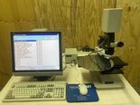
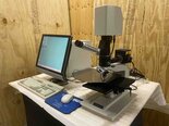
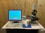
Used NANOMETRICS NanoSpec 3000 #9386854 for sale
URL successfully copied!
Tap to zoom


ID: 9386854
Wafer Size: 3"-6"
Vintage: 2001
Film thickness measurement system, 3"-6"
Solid stage linear diode array detector
(15) Standard film types
Measurement time: 0.25 sec to 4 sec
Statistical data analysis
Data export (ASCII)
Optics: 10x
Spot size: 25 μm
Computer: 333 MHz
Hard dive: 3.2 G
RAM: 64GB
Film: (3) Layers
Film thickness range: 250 A to 35 µm
Wavelength range: 480-800 nm
Reproducibility: <2 A
Lamphouse: 50 W
Power supply:
117±5% VAC, 50/60 Hz, 5 A
230 V, 50/60 Hz, 2.5 A
2001 vintage.
NANOMETRICS NanoSpec 3000 Mask and Wafer Inspection Equipment is an advanced, high resolution inspection system designed to accurately assess feature sizes and die characteristics on masks and wafers. It is used in the research and development of new products, as well as during the production of integrated circuits. NanoSpec 3000 features an air bearing based, high-resolution image acquisition and signal processing unit designed for investigating sub-micron structures on masks and wafers. The machine includes an automated vision tool that can rapidly analyze and image areas from a few microns up to several hundred microns in size. Furthermore, it is able to snap images from a variety of angles, including 75°, 60° and 45°, providing the user with a complete visual picture of the object under inspection. Unlike other inspection systems, NANOMETRICS NanoSpec 3000 also features a precision vision displacement stage that can move the specimen in x, y and z directions so that precise measurements can be made. This allows the user to manually adjust and extract precise measurement data, as well as analyze the entire die for any irregular features. The asset also has the capacity to do non-destructive wafer test and analysis. Using real-time imaging and multiple regions -of-interest selection, users can quickly access and review data on various wafer structures and components. This process can help to evaluate the integrity of any local defects and/or aberrations on the wafers under test, without disrupting the design. NanoSpec 3000 also features a high-speed real-time processing model for analyzing critical dimensions (CDs) using digital optical methods. Additionally, users can acquire sub-surface images of ICs, utilizing photo-emission microscopy, or utilize spectral measurements to analyze display parameters and test spectral changes induced by films or process parameters. Finally, the Mask and Wafer Inspection Equipment will also generate reports of the data generated during the testing. This can help with process troubleshooting and improving overall yield in the production process. In summary, NANOMETRICS NanoSpec 3000 is a powerful inspection system capable of providing complete visual analysis on both masks and wafers. It includes features like an automated vision unit, a precision vision displacement stage, non-destructive wafer test and analysis and a high-speed real-time processing machine. All of these features combined make NanoSpec 3000 an ideal choice for accurately assessing feature sizes and die characteristics on masks and wafers.
There are no reviews yet


