Used NANOMETRICS NanoSpec 4000 #6696 for sale
URL successfully copied!
Tap to zoom


ID: 6696
System
Head assy:
Photomultiplier tube
Wavelength gears
Voltage regulator PCB
Realign head optics
Computer assy: CS-9
Main power supply
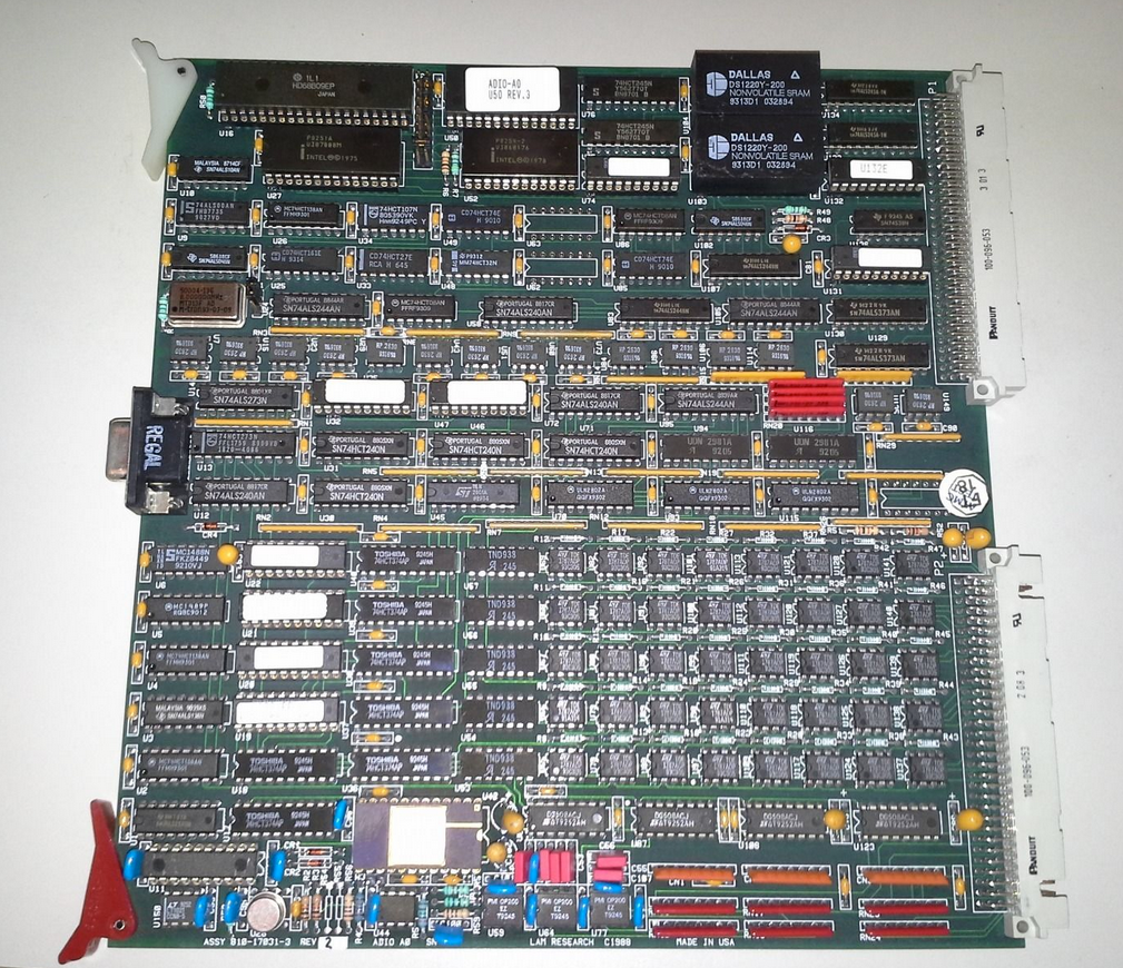
RAM/ROM PCB
R&R all PCB's
PC computer:
NANO 4000
Microscope assy:
R&R microscope stand and stage assy with focusblock
Stage addy with 6" capability
Microscope lamp
Optics 5x, 10x, and 50x (15x for UV)
Color monitor with keyboard
Optional:
8" wafer capability
Photomultiplier tube
Standard film type measured: / Typical range: / Typical repeatability:
Single layer films visible UV: / 500-50.000A, 25-500* / 2A
Triple layer films consult factory: / - / -
Single layer thick films visible: / 4 - 75 micron* / 1%
Double layer thick films consult factory: / - / -
Reflectance visible UV: / 400-850 run, 200>400nm / 0.4%, 0.2%
Oxide on poty UV: / 150-10.000A / 2A
Oxide on metal visible UV: / 3,000-20,000*, 500-5,000A / 3A, 3A
Double layer films visible:
Top layer / 100-30.000A / 2A
Bottom layer / 100-10.000X / 8A.
NANOMETRICS NanoSpec 4000 is a powerful mask and wafer inspection equipment designed to provide complete coverage of your semiconductor production process. Utilizing advanced optical imaging technology, this platform provides nanoscale accuracy and repeatability, enabling wafer and mask inspection with unparalleled accuracy and speed. The system is capable of inspecting devices ranging from 2 microns to 2 millimeters in size and can be programmed to detect and measure features having dimensions down to 10 nm in size. At its core, NanoSpec 4000 is equipped with an automated mask and wafer inspection subsystem that inspects the layout of an individual layer using a pattern recognition algorithm to compare the desired layer versus the actual layer. The unit is capable of detecting the smallest feature sizes with an extraordinary level of accuracy and repeatability, and its automated optics allow for fast, high-precision image processing in order to selectively evaluate only the desired regions of the pattern. NANOMETRICS NanoSpec 4000 also provides advanced measurement capabilities, with the platform able to capture, store, analyze, and interpret multiple surface topography parameters. Using nanoscale precision, the machine is capable of producing highly accurate surface measurements, min/max values, and surface roughness possibilities. This benefit extends to both vertical and horizontal measurements and can help manufacturers to accurately measure and diagnose any problems that arise within their wafer or mask designs. Advanced image correction and image analysis capabilities allow for accurate alignment of the mask and wafer, while true color brilliance ensures that the outputted images have bright and accurate colors. Integrated data entry, hardware/software test programming and calibration capabilities are available, along with a range of professional analysis and review tools. NanoSpec 4000 is designed to meet the quality control and inspection needs of today's high-precision manufacturing environment. Its unmatched combination of accuracy and repeatability, combined with advanced imaging and measurement capabilities, provide the assurance needed to ensure your semiconductor production is running at peak efficiency.
There are no reviews yet

